Advanced Packaging Part 3 – Intel’s Curious Bet on Thermocompression Bonding, ASM Pacific, Kulicke and Soffa, and Besi TCB Tool Landscape
In part 1 of this series, we discussed the need for advanced packaging and a basic overview. In part 2, we discussed the major types that are offered with an emphasis on logic offerings, but also delving into memory and image sensors. In part 3, we will discuss thermocompression bonding (TCB) and the 3 major tool players in this landscape, ASM Pacific, Kulicke and Soffa, and Besi. Thermocompression bonding is an evolution of the standard flip chip process, but involves many advantages and disadvantages which we will discuss here.
Thermocompression bonding (TCB) is used in all current forms of HBM memory. Most of Intel’s packaging technologies also use TCB. Intel has made a very curious bet on the technology as a driver of their packaging needs, one that TSMC has not followed suit with at all. We will discuss how this technology and Intel’s unique role in the development of it which enables them to be a leader in advanced packaging, but we will also discuss some of the drawbacks. Intel looks to continue their spending on TCB tools with hundreds of millions of dollars of orders flying in for their expansions in Arizona, New Mexico, as well as the new $7B packaging facility in Malaysia. We will first explain the technology, Intel’s major role in development of this technology, and lastly the tool ecosystem.
To understand TCB’s advantages, we must first talk the drawbacks of flip chip packaging. As discussed in part 2, the standard flip chip process starts with depositing a flux or non-conductive paste. A die placement tool then accurately places chips on a substrate, interposer, or carrier. This is done in a batch process, so that many packages can have their dies placed all at once. The set of placed dies then go off to a reflow oven or continuous reflow belt furnace, which is also a batch process. Dozens, hundreds, or even thousands of packages are put in an oven, heated up to a temperature that melts the solder to finalize the bond, then those move on to future steps such as flux residue removal and underfill.
This process is incredibly fast but comes with some major drawbacks. The largest issues are related to the coefficient of thermal expansion (CTE). Because the entire package which consists of many different materials, being heated up in a reflow oven causes these different materials to expand at different rates. This isn’t the best analogy but work with us. If you have ever baked a pie, you know the pie crust, and the filling of the pie do not expand at the same rate. If you are not careful with several different factors, your filling will end up boiling over the top layer of crust and making that crust soggy.
As the chip and substrate expand and cool, the difference in CTE can cause warpage. In addition, because dies are placed and then soldered later, the solder balls may not be making perfect contact with every copper pad causing chip gap variation. Lastly the die may not be placed perfectly flat. These minor issues can add up over time to cause early failures or worse electrical performance.
The industry can look no further than many of the original passive interposer technologies. Failure rates for AMD’s Fiji based GPUs were quite high as the process didn’t result in perfect bonds and eventually thermal cycling ended up in products not working. These reliability concerns have improved over time as TSMC and ASE/SPIL have learned how to do interposer-based packaging, but they have not been solved entirely. These issues are still relatively common in environments where temperatures are not kept stable and the package cycles between high and low temperatures frequently.
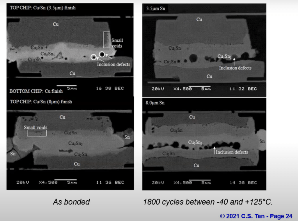
Enter thermocompression bonding. Rather than placing dies and shipping the entire assembly off to a reflow oven in batch processes, a singular tool will place individual dies, apply pressure, and heat them up to reflow the solder balls. TCB solves a few major concerns with standard flip chip. Heat is applied from the top of the chip, so only the chip and C4 solder connections heat up. This minimizes any substrate warpage issues. The force ensures even bonds with no gap variation or tilt. Lastly, when that force is applied, it can be accompanied with rapid vibration, which breaks up oxidation of metals on the copper bonding pad and solder ball. The bond that results in virtually no voids and no contamination.
TCB enables better electrical properties at the same IO pitch. TCB allows IO pitches to scale to smaller sizes. TCB also enables the packaging of thinner dies and packages. The latter is the reason HBM uses TCB and why Huawei experimented with TCB for the mobile chip market. TCB seems like an outright better technology versus the standard flip chip process flow, but that ignores one major element.
Cost.
An advanced TCB tool places on the order of 500 to 1,000 die an hour and costs ~$1.25M. An advanced flip chip die placement tool on the other hand places 3,000 to 10,000 die per hour and costs ~450k. These numbers vary widely depending on the tradeoff of accuracy versus throughput and various features that can come with the tool, but its obvious standard flip chip is much higher throughput. Reflow ovens or furnaces are very cheap and can handle the output of many die placement tools, so that cost isn’t worth worrying about.
The curious part of this is that Intel owns nearly 300 TCB tools and the Malaysia packaging facility will double that tool count. The 300 tools far outpaces Intel’s advanced packaging uses. Intel uses TCB in many non-advanced packaging applications where the standard flip chip process would be perfectly fine. SemiAnalysis spoke with an Intel packaging engineer off the record, and the rationale was quite interesting. Given Intel’s heavy share in high power and high margin applications, the yield loss and reliability concerns far outweigh the miniscule, amortized cost of the tool per unit packaged.
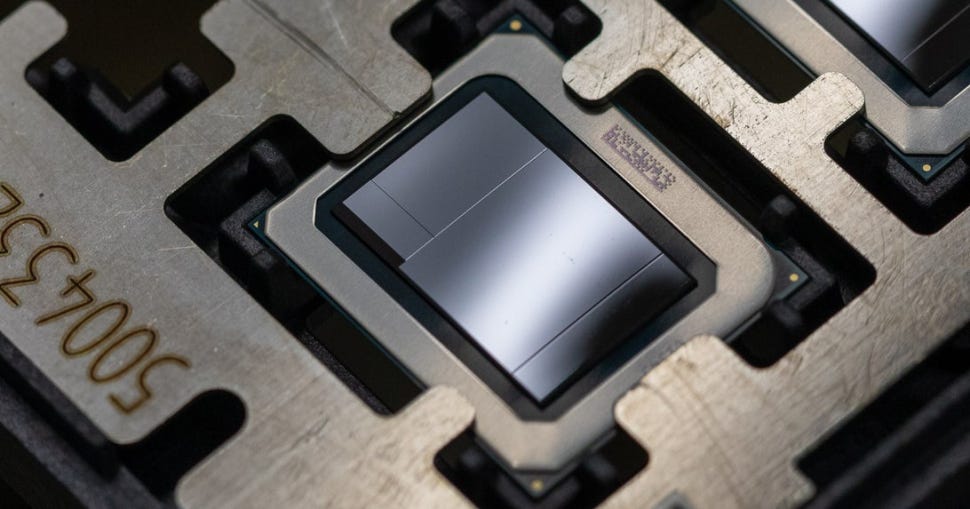
Furthermore, these tools give a lot of flexibility related to type of packaging. Intel can use the same tool for standard packages, 2.5d packages, and advanced 3d packaging. The above image is from der8auer, and it showcases an Intel Sapphire Rapids server CPU with multiple pitch sizes. There is a section that is 55-micron pitch for EMIB, and 100-micron pitch for the rest of the die to package connection. While this is theoretically possible without TCB, the implementation in the real world is much easier given the differences in size of pads and solder caps.
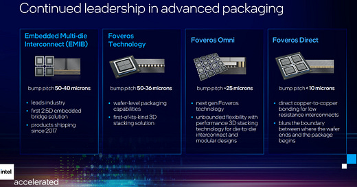
The capabilities of TCB really start to shine when Intel moves to Foveros Omni. We discussed the technology more in part 2, but the copper pillars and ODI dies make Foveros Omni neigh on impossible to package with the standard flip chip process. The first Foveros Omni product will be Intel’s Meteor Lake, a mass market client architecture designed for 5W SOCs all the way up through high power desktops. (Edit: This was redefined to be Arrow Lake) Despite including many die, Omni enables large cost savings on manufacturing cost, selecting the optimal process node for IP and minimize die sizes to enhance yields. The package has various bump pitches from 130-micron, 100-micron, and 36-micron. Advanced 3D logic packaging isn’t only for the high performance applications.
TSMC, Samsung, and many others will not be able to do this sort of packaging unless they invest heavily in TCB. Intel has been co-developing TCB tools for over a decade, so it would be hard for competitors to instantly to move towards this technology. InFO from TSMC utilizes standard flip chip flows while potentially being a more costly packaging technology due the more expensive substrate. TSMC hasn't advanced packaging but on commodity standard ABF substrates, which is a hinderance in how far down they can bring advanced packaging in terms of cost. At the same time, InFO does have some major advantage which we discussed in part 2, namely related to complex routing within the RDL without the use of silicon dies. TSMC does use TCB for HBM, but that is a very different niche than logic stacking.
Hybrid bonding is capabilities beyond anything flip chip TCB can offer, but that technology operates at a completely different point on the cost and performance curve, which diminishes its ability to ramp in volume for the medium term. This will be discussed in part 4. Intel’s embrace of TCB has enabled them to create optionality’s around various IP and have many different blocks fabbed on many different nodes without a large penalty in die-to-die connections. The specifics about the strategy on design side are discussed in this article about the Intel TSMC wafer supply agreement article.
TCB has also been adopted in HBM applications as well. HBM dies need to be extremely thin. The image above is only memory 4 stacks, but as the industry scaled to 8 stacks and beyond, it has become mandatory for Samsung, SKHynix, and Micron to use TCB. In SKHynix’s upcoming 12 stack HBM3, the demands of die thinness have become so extreme, each die is thinned to 30-microns. The bump pitch is similarly, incredibly dense. The only way to enable HBM stack is with TCB technologies currently, but the industry looks forward to potentially using more exotic forms of packaging such as hybrid bonding.
Due to being the best technology for packaging extremely thin die, TCB was also experimented with by mobile phone applications that shipped in flagship devices using packaging by both OSATs and IDMs. Samsung, Qualcomm/Amkor, and Huawei/ASE have used TCB in some applications related to package on package (PoP) DRAM. OSATs are beginning to order more and more TCB tools, but the largest orders are still from Intel with their custom co-developed TCB platforms. The important things to note about these other use cases is that they aren’t the same tools as Intel’s and they aren’t designed for high power or performance applications.
The market between ASM Pacific, Kulicke and Soffa, and Besi is quite dynamic for TCB and each one excels in different areas. This has resulted in each having their own niche. Order books are going up in a major way, but not consistently across the 3 due to the niches they each occupy.
We will discuss this in the subscriber only section.


