Advanced Packaging The Size Of Your Monitor | Applied Materials, $AMAT, Modifies Panel PVD Tool For 60x60cm Fan Outs To Usher In A New Age Of Mega Packages
Applied Materials has been working hard on modifying a physical vapor deposition tool in order to enable panel level packaging. This tool originates from their acquisition of Tango Systems. It is the convergence of techniques used for LCD panel, Printed Circuit Board technologies, and Fan Out Wafer Level packaging such as that used on the Dojo chip. Applied Materials claims it can do this with less than half the normalized capital costs compared to wafer level packaging.
As you can see these packages are massive and dwarf anything we see in chips today. It would allow the packaging of dozens, if not over a hundred different chips. The Applied Materials promo states 600mm by 600mm packages, but older details of this tool mention 670mm by 580mm. Regardless, a package around 34 inches in diagonal is mindboggling.
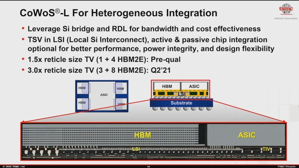
It can deposit layers as thin as 10um and do interconnect layers, low resistance contacts, or conformal seed layers for etched or laser drilled vias. This technology supports embedded die in substrate technologies such as Intel’s EMIB (embedded multi-die interconnect bridge) or TSMC’s LSI (local silicon interconnect). In addition, it can be used on organic and glass interposers.
The new PVD tool doesn’t come alone and comes with a combination of Applied Materials capabilities from its Display Group, including deposition, eBeam testing, SEM review and metrology, and focused ion beam for defect analysis. We are excited to see if this will be used in mega packages. Initial use cases will be as a cost optimization point for running many packages and individual products at once, but it was made clear that this is just the start.
This article was originally published on SemiAnalysis on September 12th 2021.
Clients and employees of SemiAnalysis may hold positions in companies referenced in this article.


