AI Capacity Constraints - CoWoS and HBM Supply Chain
Quarterly Ramp for Nvidia, Broadcom, Google, AMD, AMD Embedded (Xilinx), Amazon, Marvell, Microsoft, Alchip, Alibaba T-Head, ZTE Sanechips, Samsung, Micron, and SK Hynix
Generative AI is upon us and it will change the world. Ever since ChatGPT took the world by storm and captured our imaginations about the possibilities of AI, we are seeing all sorts of companies rushing to train AI models and deploy generative AI into internal workflows or customer-facing applications. It’s not just big tech and startups, many non-tech fortune 5,000 companies are figuring out how to deploy LLM-based solutions.
Of course, this will require massive amounts of GPU compute. GPU sales are going up like a rocket and the supply chain has struggled to keep up with the demand for GPUs. Companies are scrambling to get their hands on GPUs or cloud instances.
Even OpenAI can’t get enough GPUs and this is severely bottlenecking its near-term roadmap. OpenAI cannot deploy its multi-modal models due to GPU shortages. OpenAI cannot deploy longer sequence length models (8k vs 32k) due to GPU shortages.
Meanwhile, Chinese companies are not only investing to deploy their own LLMs but also stocking before US export controls tighten even further. For example, Bytedance, the Chinese company behind Tik Tok is supposedly ordering over $1B worth of A800/H800s from Nvidia.
While there are many legitimate use cases for hundreds of thousands of GPUs dedicated to AI, there are also many cases where people are rushing to buy GPUs to try to build something they aren’t sure has a legitimate market. In some cases, big tech firms are trying to catch up to OpenAI and Google, so as not to be left in the dust. There is a flood of VC money to startups that have no proven business use case. We know of over a dozen enterprises that are trying to train their own LLM on their own data. Lastly, this also applies to nation states with both Saudi Arabia and the UAE also attempting to acquire hundreds of millions of dollars of GPUs this year.
The highest-end Nvidia GPU, H100, will remain sold out until Q1 of next year, despite Nvidia’s attempts to increase production drastically. Nvidia will be ramping to ship more 400,000 H100 GPUs per quarter.
Today we will detail the bottlenecks to production and how much downstream capacity is expanding for Nvidia and their competitors. We will also share our estimates for the the supply increases by quarter for Nvidia, Broadcom, Google, AMD, AMD Embedded (Xilinx), Amazon, Marvell, Microsoft, Alchip, Alibaba T-Head, ZTE Sanechips, Samsung, Micron, and SK Hynix.
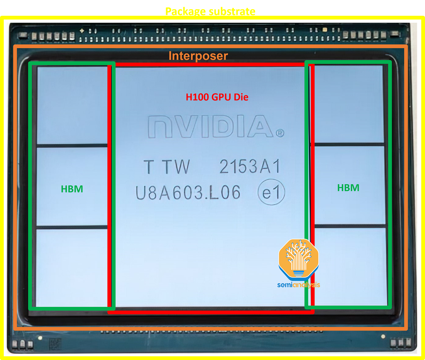
Nvidia’s H100 is 7-die packaged on CoWoS-S. In the center is the H100 GPU ASIC which has a die size of 814mm2. Surrounding it are 6 stacks of memory, HBM. The HBM configuration changes between various SKUs but the H100 SXM version uses HBM3, with each stack being 16GB for 80GB total memory, only 5 HBM are used and a dummy die. The H100 NVL will have two packages with 6 active stacks of HBM on each package.
In cases where there are only 5 active HBM, the non-HBM die can dummy silicon which is there to provide structural support for the chip. These die sit atop a silicon interposer that is not clearly visible in the picture. This silicon interposer sits on a package substrate which is an ABF package substrate.
The GPU Die and TSMC Fabrication
The main number-crunching component of Nvidia’s GPUs is the processor die itself, fabricated on a customized TSMC process node called “4N.” It is fabricated in TSMC’s Fab 18 in Tainan, Taiwan, sharing the same facilities as TSMC N5 and N4 process nodes. This is not a limiting factor to production.
TSMC’s utilization rates for the N5 process node fell below 70% due to massive weakness in PC, smartphone, and non-AI related datacenter chips. Nvidia has had no problem securing additional wafer supply.
In fact, Nvidia has ordered a large number of wafers for H100 GPUs and NVSwitch that started production immediately, well before they are required for shipping chips. These wafers will sit at TSMC’s die bank until the downstream supply chain has enough capacity to package these wafers into completed chips.
Basically, Nvidia is soaking up some of TSMC’s low utilization rates and getting a bit of a pricing benefit because NVIDIA has committed to purchase the finished product further down the road.
A wafer bank, also known as a die bank, is a practice in the semiconductor industry where partially processed or completed wafers are stored until they are needed by the customer. Unlike some other foundries, TSMC will help their customers by keeping these wafers on their own books almost fully processed. This practice allows TSMC and its customers to maintain financial flexibility. As they are only partially processed, wafers held in the wafer bank are not considered finished goods, but instead are classified as WIP. It is only when these wafers are fully completed that TSMC can recognise revenue and transfer ownership of these wafers to their customers.
This helps customers dress up their balance sheet so it appears that inventory levels are under control. For TSMC, the benefit is that it can help keep their utilization rates higher which supports margins. Then, as the customer needs more inventory, these wafers can be fully completed by a few final processing steps and then delivered to the customer at the normal sales price or even a slight discount.
The Emergence of HBM in the Datacenter: How AMD's Innovation Aided Nvidia
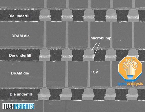
The High Bandwidth Memory around the GPU is the next major component. HBM supply is also limited, but ramping. HBM is vertically stacked DRAM dies connected via Through Silicon Vias (TSVs) and bonded using TCB (hybrid bonding will be required for higher stack counts in the future). Beneath the DRAM dies sits on a base logic die that acts as a controller. Typically, modern HBM has 8 layers of memory and 1 base logic die but we will see products with 12+1 layer HBM soon, for example AMD’s MI300X and Nvidia’s upcoming H100 refresh.
Interestingly, it was AMD that pioneered HBM, despite Nvidia and Google being the highest volume user today. In 2008, AMD predicted that the continual scaling of memory bandwidth to match gaming GPU performance would need more and more power that would need to be diverted away from the GPU logic and therefore detract from GPU performance. AMD partnered with SK Hynix and other companies in the supply chain (such as Amkor) to find a memory solution that would deliver high bandwidth with lower power. This resulted in the development of HBM in 2013 by SK Hynix.
SK Hynix first shipped HBM in 2015 for AMD’s Fiji series of gaming GPUs which was 2.5D packaged by Amkor. This was followed up with the Vega series in 2017, which used HBM2. However, HBM wasn’t much of a game-changer for gaming GPU performance. With no clear performance benefits coupled with higher cost, AMD returned to using GDDR for its gaming cards after Vega. Today, top of the line gaming GPUs from Nvidia and AMD are still using cheaper GDDR6.
However, AMD was somewhat correct with their initial prediction: scaling memory bandwidth has proven to be a problem for GPUs, just that it is a problem mostly for datacenter GPUs. With consumer gaming GPUs, Nvidia and AMD have turned to large caches for the frame buffer, enabling them to stay with much lower bandwidth GDDR memory.
As we have detailed in the past, inference and training workloads are memory intensive. With the exponential rise in the number of parameters in AI models this is pushing model size to terabytes for weights alone. Therefore, AI accelerator performance is bottlenecked by the ability to store and retrieve training and inference data from memory: a problem often known as the memory wall.
To address this, leading-edge datacenter GPUs are co-packaged with High Bandwidth Memory (HBM). Nvidia released their first HBM GPU, the P100 in 2016. HBM tackles the memory wall by finding a middle ground between conventional DDR memory and on-chip cache, trading capacity for bandwidth. Much higher bandwidth is achieved by drastically increasing pin counts to reach a 1024 bit wide memory bus per HBM stack, which is 16x that of DDR5 at 64 bit width per DIMM. At the same time, power is kept in check with drastically lower energy per bit transfer (pJ/bit). This is achieved through much shorter trace lengths, which measure in millimetres for HBM vs cm for GDDR and DDR.
Today, many HPC-facing chip companies are enjoying the fruit of AMD’s efforts. Ironically, AMD’s rival Nvidia has perhaps stood to benefit the most as the highest volume user of HBM.
The HBM Market: SK Hynix Dominance | Samsung And Micron Investing To Catch Up
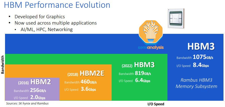
As the pioneer of HBM, SK Hynix is the leader with the most advanced technology roadmap. SK Hynix started production of HBM3 in June 2022 and is currently the only supplier shipping HBM3 in volume, with over 95% market share, which is what most H100 SKUs are using. The max configuration of HBM now 8-layer 16GB HBM3 modules. SK Hynix is producing 12-layer 24GB HBM3 with a datarate of 5.6 GT/s for the AMD MI300X and Nvidia H100 refresh.
The main challenge with HBM is packaging and stacking the memory, which is what SK Hynix has excelled at, having accumulated the strongest process flow knowledge. In another post, we also detailed how SK Hynix’s 2 key packaging innovations are beginning to ramp up and will displace one key equipment vendor in the current HBM process.
Samsung is next behind Hynix and expects to ship HBM3 in the second half of 2023. We believe they are designed for both Nvidia and AMD GPUs. They currently have a big deficit in volume to SK Hynix, but they are hot on the trails and are investing hugely to catch up on market share. Samsung is investing to catch up and become number 1 in HBM market share just like they are with standard memory. We hear they are cutting favorable deals with some of the accelerator firms to try to capture more share.
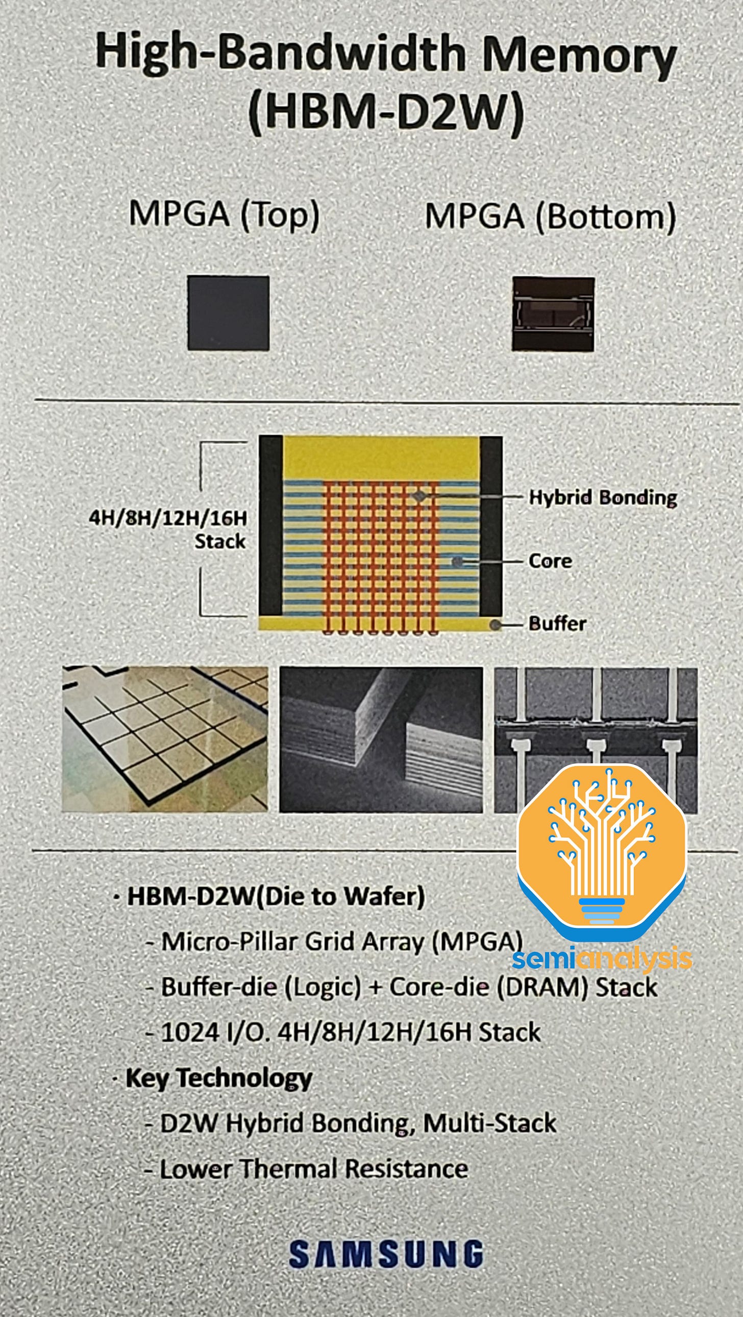
They have shown off their 12-layer HBM as well as future Hybrid Bonded HBM. One interesting aspect of Samsung’s HBM-4 roadmap is that they want to make the logic/periphery on an in-house FinFET node. This shows the potential advantage they have of having logic and DRAM foundry in house.
Micron is the furthest behind. Micron was more heavily invested in Hybrid Memory Cube (HMC) technology. This was a competing technology to HBM with a very similar concept that developed around the same time. However, the ecosystem around HMC was closed, making it difficult for IP to be developed around HMC. Furthermore, there were some technical deficiencies. Adoption for HBM was much higher so HBM won out to become the industry standard for 3D stacked DRAM.
It was only in 2018 that Micron started to pivot away from HMC and invest into HBM roadmap. This is why Micron is the furthest behind. They are still stuck on HBM2E (which SK Hynix started mass producing in the middle of 2020) and cannot even manufacture top bin HBM2E successfully.
In their most recent earnings call Micron made some bold statements about their HBM roadmap: they believe they will go from laggard to leader with their HBM3E in 2024. HBM3E is expected to start to ship in Q3/Q4 for Nvidia’s next generation GPU.
Our ramp of HBM3, actually the sort of the next generation of HBM3, which is a much higher level of performance, bandwidth and lower power than what is in production in HBM3 today in the industry. That product, our industry-leading product will be ramping in volume starting CQ1 of 2024, and will be meaningful in revenue for fiscal year '24 and then substantially larger in 2025, even from those 2024 levels. And we will -- we are targeting a very robust share in HBM higher than unnatural supply share for DRAM in the industry.
Sumit Sadana, Micron Chief Business Officer
The statement that they will have higher market share in HBM versus their general DRMA marketshare is very bold. Given they still struggle to manufacture top bin HBM2E at high volume, we find it hard to believe Micron’s claim that they will ship leading edge HBM3 in early 2024 and even be the first to HBM3E. It feels to us as though Micron is trying to change the narrative away from being an AI loser despite dramatically lower memory content per Nvidia GPU server versus Intel/AMD CPU server.
All our channel checks see SK Hynix remaining strongest at new-generation technologies and Samsung trying very hard to catch back up with huge supply increases, a bold roadmap, and cutting deals.
The Real Bottleneck - CoWoS
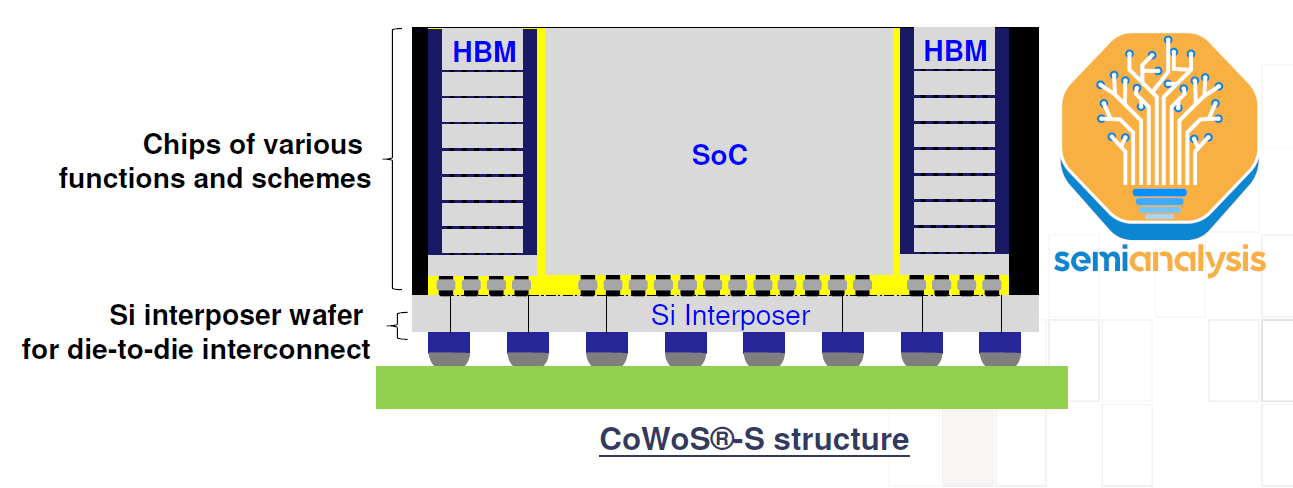
The next bottleneck is CoWoS capacity. CoWoS (Chip on Wafer on Substrate) is a “2.5D” packaging technology from TSMC where multiple active silicon dies (the usual configuration is logic and HBM stacks) are integrated on a passive silicon interposer. The interposer acts as a communication layer for the active die on top. The interposer and active silicon are then attached to a packaging substrate which contains the I/O to place on the system PCB.
HBM and CoWoS are complementary. The high pad count and short trace length requirements of HBM necessitate 2.5D advanced packaging technologies like CoWoS to enable such dense, short connections that can't be done on a PCB or even a package substrate. CoWoS is the mainstream packaging technology that offers the highest interconnection density and largest package size with reasonable costs. As almost all HBM systems are currently packaged on CoWoS, and all advanced AI accelerators use HBM, the corollary is that virtually all leading-edge data center GPUs are packaged on CoWoS by TSMC. Baidu does have some advanced accelerators with Samsung on their version.
While 3D packaging technologies such as TSMC's SoIC enable stacking dies directly on top of logic, it does not make sense for HBM due to thermals and cost. SoIC sits on a different order of magnitude regarding interconnect density and is better suited to expanding on-chip cache with die stacking, as seen with AMD's 3D V-Cache solution. AMD’s Xilinx was also the first users of CoWoS many years ago for combining multiple FPGA chiplets together.
While there are some other applications that use CoWoS like networking (and some of these are adopted for networking GPU clusters like Broadcom’s Jericho3-AI), supercomputing, and FPGAs, the vast majority of CoWoS demand comes from AI. Unlike other parts of the semiconductor supply chain, where weakness in other major end markets means there is plenty of slack to absorb the enormous pickup in GPU demand, CoWoS and HBM are already majority AI-facing technologies, so all slack was already absorbed in Q1. With GPU demand exploding, these are the parts of the supply chain that just cannot keep up and are bottlenecking GPU supply.
Just recently in these 2 days I received a customer's phone call requesting a big increase on the backend capacity, especially in the CoWoS. We are still evaluating that.
C.C Wei, TSMC CEO
TSMC has been getting ready for more packaging demand but probably did not expect this wave of generative AI demand to come so quickly. In June, TSMC announced they have opened their Advanced Backend Fab 6 in Zhunan. This fab has an area of 14.3 hectares which would be enough cleanroom space for potentially 1 million wafers per year of 3D Fabric capacity. This includes not only CoWoS but also SoIC and InFO technologies. Interestingly this fab is larger than the rest of TSMC’s other packaging fabs combined. While this is just cleanroom space and far from fully tooled to actually provide that much capacity, it’s clear that TSMC is getting ready in anticipation of more demand for its advanced packaging solutions.
What does help a little is there is slack in Wafer Level Fan-Out packaging capacity (primarily used for smartphone SoCs), and some of this can be repurposed in some CoWoS process steps. In particular, there are some overlapping processes such as deposition, plating, back grinding, molding, placement, and RDL formation. We will go through the CoWoS process flow and all the firms who see positive demand due to it in a follow-up piece. There are meaningful shifts in the equipment supply chain. Edit: Here is the follow up piece.
There are other 2.5D packaging technologies from Intel, Samsung and OSATs (like FOEB from ASE), CoWoS is the only one being used in high volume given TSMC is by the far most dominant foundry for AI accelerators. Even Intel Habana’s accelerators are fabricated and packaged by TSMC. However, some customers are seeking alternatives to TSMC which we will discuss below. See our advanced packaging series for more info.
CoWoS Variants
There are a few variants of CoWoS but the original CoWoS-S remains the only configuration in high volume production. This is the classic configuration as described above: logic die + HBM die are connected via a silicon-based interposer with TSVs. The interposer then sits on an organic package substrate.
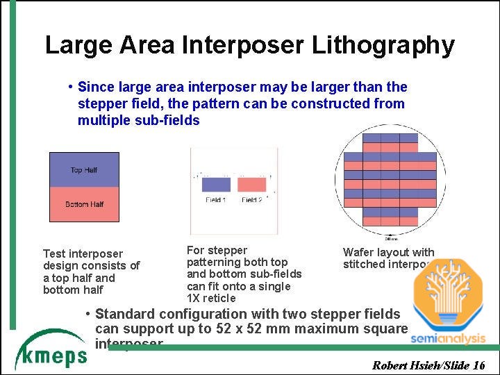
An enabling technology for silicon interposers is a technology called “reticle stitching”. Chips generally have a maximum size of 26mm x 33mm due to lithography tools slit/scan maxing out that size. With GPU die alone approaching this limit and the need to fit HBM around it too, interposers need to be large and will go well beyond this reticle limit. TSMC addresses this with reticle stitching which allows them to pattern interposers multiple times the reticle limit (as of now up to 3.5x with AMD MI300).
CoWoS-R uses on organic substrate with redistribution layers (RDLs) instead of a silicon interposer. This is a lower cost variant that sacrifices I/O density due to using an organic RDL instead of a silicon-based interposer. As we have detailed, AMD’s MI300 was originally designed on CoWoS-R but we believe due to warpage and thermal stability concerns AMD has to instead use CoWoS-S.
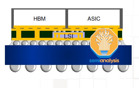
CoWoS-L is expected to ramp later this year and utilises an RDL interposer but contains an active and/or passive silicon bridge used for die-to-die interconnect that is embedded inside the interposer. This is TSMC’s equivalent to Intel’s EMIB packaging technology. This will allow for larger package sizes as silicon interposers are getting harder to scale. The MI300 CoWoS-S may be near the limit for a single silicon interposer.
It will be far more economical for even larger designs to go with CoWoS-L. TSMC is working on a CoWoS-L super carrier interposer at 6x reticle size. For CoWoS-S, they have not mentioned anything beyond a 4x reticle. This is because of fragility of the silicon interposer. This silicon interposer is only 100 microns thick and is at risk of delaminating or cracking as interposers scale to larger sizes during the process flow.
CoWoS Customers
Note the chart is not to scale or percentage, we offer our model with actual units.
For subscribers, we will walk through demand for each CoWoS company: Nvidia, Broadcom, Google, AMD, AMD Embedded (Xilinx), Amazon, Marvell, Microsoft, Alchip, Alibaba T-Head, and ZTE Sanechips.


