Apple A15 Die Shot and Annotation - IP Block Area Analysis
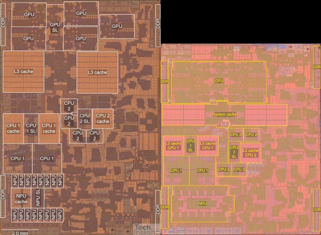
TechInsights released a die shot of the A15 and with the help of SkyJuice’s, we are analyzing it today. The total die has increased significantly in size to 107.7mm^2 from 87.76mm^2 and from 11.8B transistors to 15B transistors. The initial Apple claims were not that impressive. The most disappointing aspect was the lack of CPU gains. Despite this, there are still many changes this generation. AnandTech has done their preliminary review on the A15 SOC and combined with the die analysis many interesting details can be gleaned.
The first detail that can be confirmed is that the process density is unchanged. The individual SRAM cells are unchanged and LPDDR4x PHYs are also identical in size. This likely confirms that Apple is using N5P and not the N4 process like some speculated.
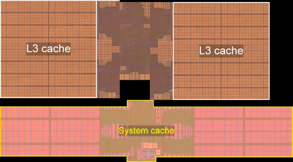
Total die area is up 22.8%, but various IP blocks differ. The shared level cache is the single largest contributor. The ISP looks highly revised as well, but we do not have measurements here. The NPU remains 16 Cores, but the cores and shared logic were changed architecturally to bring about a sizable performance increase. Despite the lack of IPC gains in the big core, the big core still has some changes.
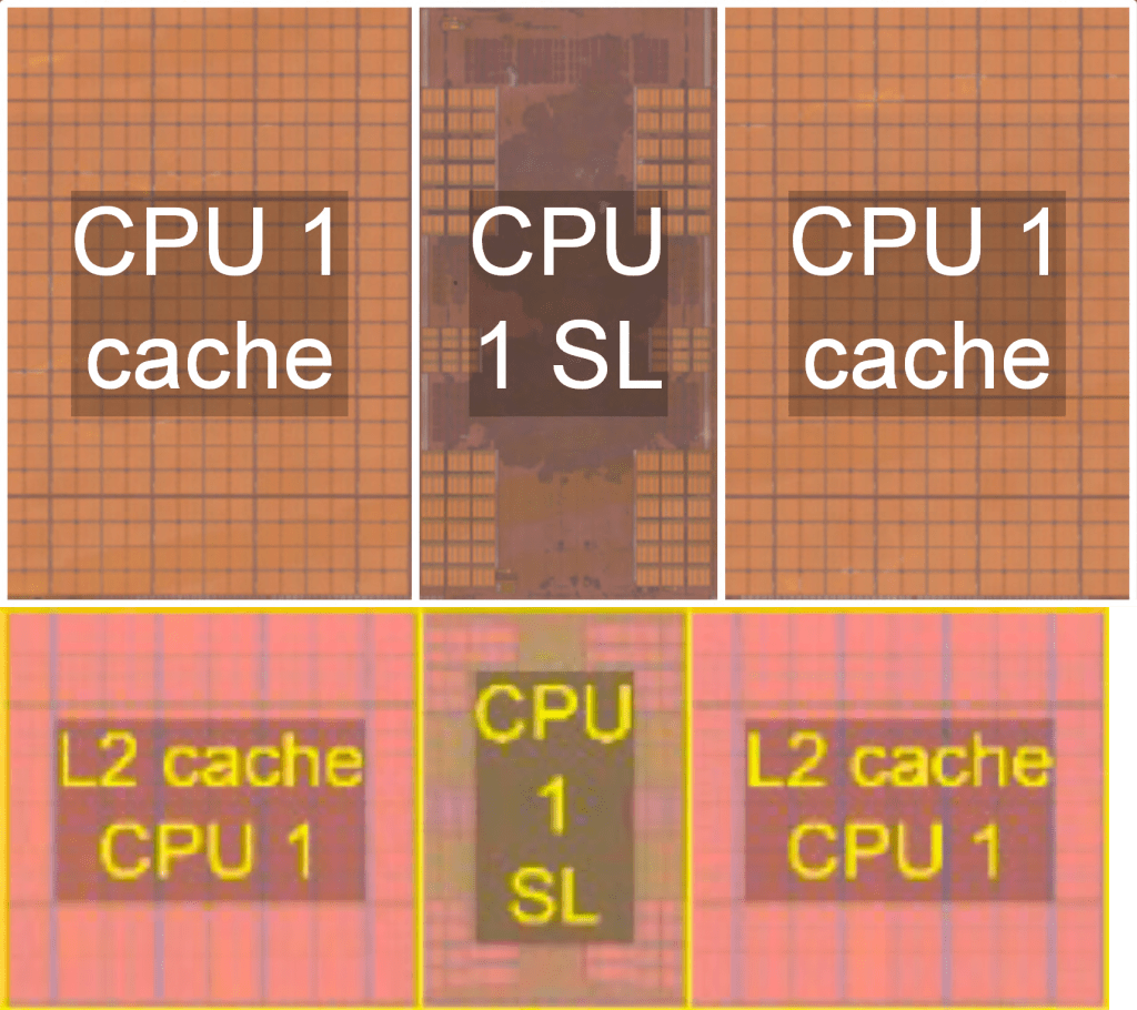
Despite being the smallest IPC gain for Apple ever, the core is clearly rearchitected. The two largest changes are related to the MMU and caches. The layout is significantly different and there is a 15.26% increase in the Core+L1 area. Anandtech discovered an interesting change to the L1 cache.
On the performance cores I’m also seeing some changes in the L1 speeds as it seems to be able to make 1-cycle accesses to cache lines, as long as they’re in the same page, the same type of access on the A14 takes 3 cycles.
The shared L2 cache was increased to 12MB from 8MB. This is identical to the M1 despite having half the cores. Anandtech found that it the access latency has increased to 18 cycles from 16. The tradeoff on size versus latency seems to be well worth it. The shared L2 cache block has grown 52% in size versus the A14.
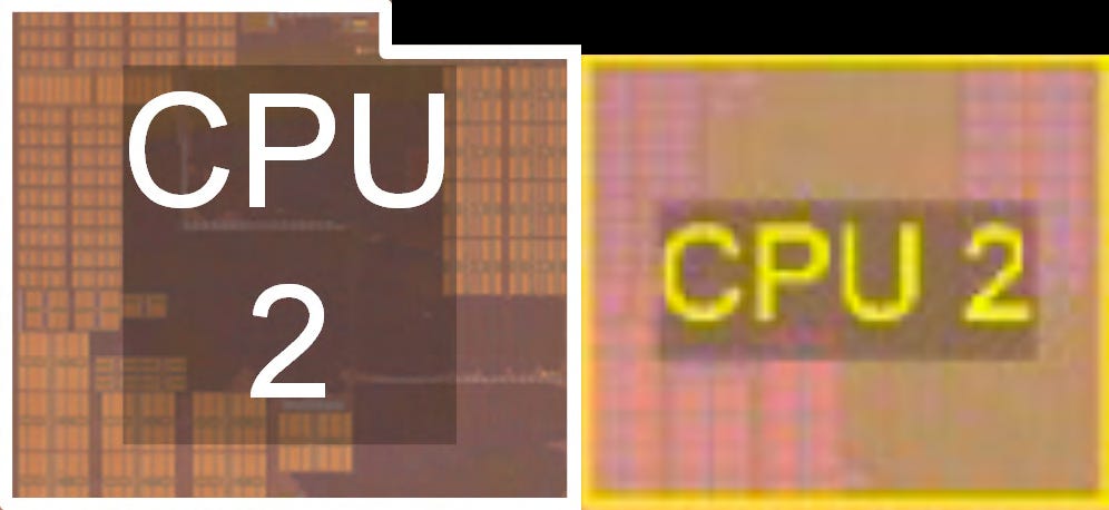
The little core, Blizzard, has grown 18.6% in size, but the performance increase is 23%. The L2 core remains 4MB, but has increased slightly by 2.5%. The Apple blizzard core is now performing on par with the big A76 core in 2 year old Android SOCs.
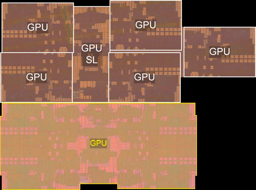
Apple really focused on GPU for the A15. Apple released this video which details some of the architectural changes. Among them is doubling the FP32 ALUs which was in the M1 GPU core. Apple also introduced lossy renderable textures that save memory storage & bandwidth, support for sparse depth & stencil textures and a new SIMD shuffle and fill instructions. Despite all of these changes, the core has only increased 4.4% in size.
The entire GPU is up 30% in size. This is mostly due to the 5th GPU core and changes to the shared logic. Even when the 5th core is disabled, there is still a sizable performance increase. The new larger GPU achieves a huge performance increase despite no increase in memory bandwidth. Apple is pursing a similar strategy to AMD’s Infinity Cache it seems.
The single largest area contributor is the system cache. It has doubled from 16MB to 32MB. This helps keep the various IP blocks of the A15 fed. This article was just a short summary of SkyJuice die analysis. What else did you folks notice about the die shot?
This article was originally published on SemiAnalysis on September 30th 2021.
Clients and employees of SemiAnalysis may hold positions in companies referenced in this article.


