ASML Dilemma: High-NA EUV is Worse vs Low-NA EUV Multi-Patterning
Cost model for low- & high-NA EUV, Feature Fidelity, Technical Challenges
This post was primarily authored by Jeff Koch, who joined SemiAnalysis last month from ASML, and will be leading our semiconductor capital equipment & manufacturing analysis. “Lithos Graphien,” an anonymous contributor with decades of experience in the chip & litho industry also helped significantly, follow him!
In recent years, the “next big thing” in photolithography has been High Numerical Aperture Extreme Ultraviolet, IE high-NA EUV, the next evolutionary step in lithography tool technology development at ASML. High-NA is marketed as reducing process complexity and enabling scaling beyond 2nm. The implication from ASML is that reduced complexity results in lower costs.
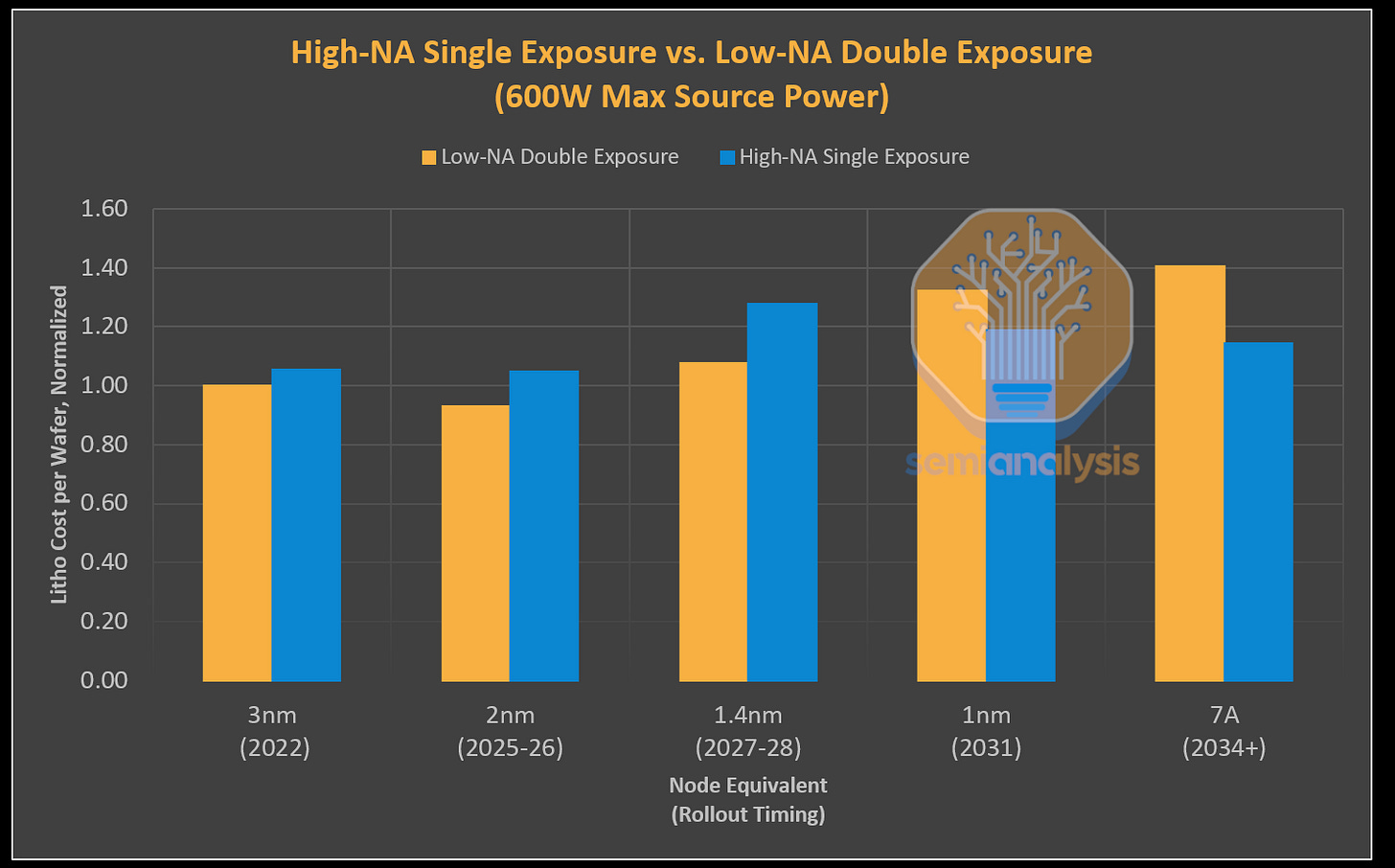
Our lithography models show that despite reducing complexity, high-NA EUV single patterning costs significantly more than double-patterning using existing low-NA machines for upcoming technology nodes including 1.4nm/14A. Furthermore, multi-patterning low-NA EUV is capable of finer pitch features than high-NA.
ASML has many lofty goals such as hitting 600 DUV and 90 EUV tool annual shipments by 2025, but the most lofty, and in our view, impossible to hit target of theirs is the plan to have 20 High-NA EUV tool annual shipments by 2028. High-NA lithography introduces many new technological challenges that need to be solved and industrialized, but the most difficult challenge is economic. Before we detail the cost and other key issues below, let’s briefly mention a similar scenario that happened with EUV and DRAM.
For most of the last two decades, Samsung has been ahead on DRAM technology, with a clear advantage on density, performance, and cost scaling versus competitors such as Micron and SK Hynix. This all changed with the D1Z generation of DRAM as Samsung adopted EUV far too quickly (among other issues) and suffered. They were not able to Micron were able to race ahead in density and cost structure due to Samsung’s stumbles. To this day, despite having fully adopted EUV now, Samsung is still behind in the density and performance race. Micron, despite using DUV, has the world’s densest DRAM by a fairly sizable margin. For more details of Samsung’s issues, see here.
Let’s be clear though, high-NA’s economic challenges are much more severe than those that low-NA’s even though the technical challenges are arguably smaller.
High-NA Development Compromises
Without rehashing the details of EUV lithography (see our previous notes on EUV background, Challenges for EUV, Chiplet vs. Large Die Conundrum, Semiconductor Supply Chains, Long-Term Wafer Demand, ASML Long-Term Outlook, Lithography Export Restrictions, and Austria's Mask Writer Monopoly) indulge us in a short history of the decisions that led to high-NA as it exists today.
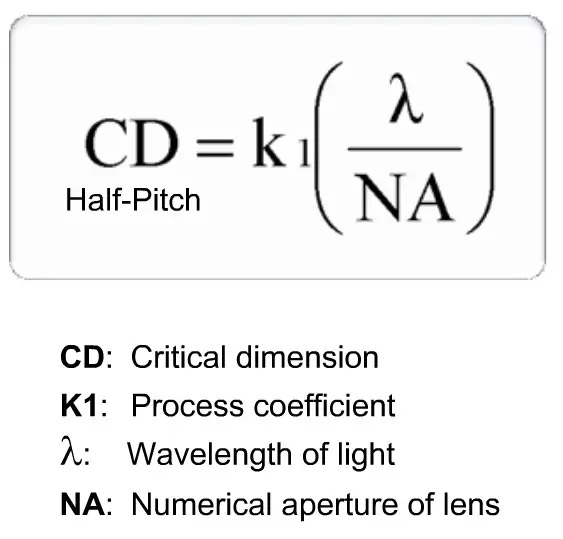
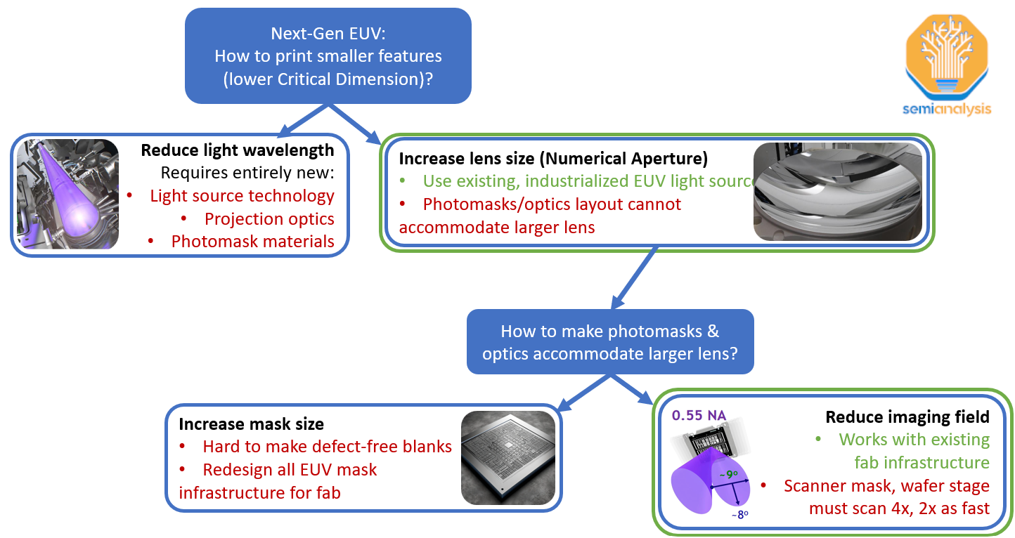
To continue logic and memory node shrink, lithography tools (scanners) must be able to print ever smaller features. At the start of high-NA development, chipmakers and ASML were faced with a difficult architectural decision on how to enable this. Fundamentally there are 2 main knobs in scanner design to image smaller features: 1) decrease the wavelength of the light source 2) increase the size of the lens (or more precisely, the numerical aperture or NA of the lens). This choice expressed as the 1st Rayleigh criterion, so ubiquitous that ASML even had t-shirts printed with it.
For numerous valid technical reasons, the industry chose to pursue larger projection lenses. Unfortunately, the lens size cannot be made larger without causing other issues, mainly due to limitations in EUV photomask technology as it relates to the chief-ray-angle. This forced further compromises in the high-NA architecture.
ASML and partners were faced with a set of poor choices:
Increase the size of the photomask, which contains the pattern to be printed on the wafer.
Decrease the size of the imaging field
The first option would not only be a massive technical challenge but also incur many knock-on effects as current mask infrastructure is designed around the standard 6” square reticle infrastructure. Producing defect free mask blanks even at current size was an obstacle in low-NA development and would not be simple to scale up to 2x or 4x in area. Actinic mask inspection tools, using low-power EUV light sources to inspect EUV masks, only recently became available and are designed around the 6” standard. EUV masks and infrastructure are already multiple times more expensive than the DUV equivalents and the cost of increasing area scales rapidly.
Option 2 seemed to be the lesser of 2 evils. While it also introduced serious technical challenges, it did not require significant changes to the lithography ecosystem outside the scanner. Chipmakers threw their weight behind this second option and ASML embarked on development work that will culminate shortly in the shipment of the first high-NA machine, the EXE:5000.
These architectural decisions have a few key implications: technical challenges with half-field stitching, depth of focus, and photoresist, and cost challenges when compared to the existing low-NA tools. We’ll explore each of these in turn.
Half-Field Challenges
Lithography scanners expose wafers through an exposure slit. The wafer is moved, or scanned, under the slit in order to expose the pattern from the photomask onto the wafer. Once the entire mask pattern has been exposed, the scanner steps over to a fresh area of the wafer and repeats the scan. The exposure field is the area covered by a single full exposure of the mask.
You can see this step-and-scan motion in the gif from ASML below. Remember that the movement is fast enough to cover hundreds of wafers per hour and with pattern placement accuracy down to the nanometer level, near atomic level – it’s incredible that it works.
The exposure field size for high-NA scanners is only half that of low-NA EUV and traditional DUV tools. This was the “lesser of 2 evils” tradeoff that allowed for the lens size to increase while maintaining the industry standard photomask dimensions.
One of the “evils” in this tradeoff was the necessity of mixing half- and full-field exposures on the same wafer. High-NA will only be used on a few of the most critical layers, i.e. those with the smallest features to be printed. Cheaper tools with relaxed imaging capabilities will be used for the others. This means that mask layouts and chip dimensions must be planned with both half-field and full-field imaging in mind. Given that even without the added complication of half-field, poorly optimized mask layouts can lead to high costs despite small die sizes, this will certainly be an issue for future chip designs.
There are a lot more issues at play here, and chip designers should be keenly aware, but we will dive into those at the end of this report. Onto the primary topic, costs and feature fidelity.
Dose vs. Throughput
To understand the cost implications of the high-NA architecture, we need to baseline the concepts of scanner exposure dose and its effect on throughput. Lithography cost is dominated by the lithography tool (scanner) cost. The newest low-NA NXE:3800E tools now cost more >$200M each, and as such, the cost of the scanner per wafer produced is dominated by a scanner’s throughput.
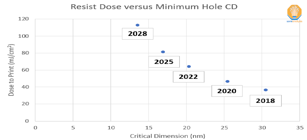
Dose is a measure of energy reaching the wafer. This energy generates a chemical reaction in the photoresist that changes it from insoluble to soluble, or vice versa. Patterning smaller features generally requires a higher dose to avoid a variety of errors. Crucially, the dose requirements increase exponentially for decreasing CD.
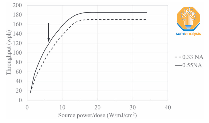
Why does this matter? Because dose affects throughput and therefore cost. A higher dose requires either
A more powerful light source
Slowing down the scanner
ASML has been reliably increasing source power with each new EUV model, but not enough to keep up with exponentially rising dose requirements. This means the scanner must slow down so that each exposure field receives at least the minimum dose.
Put simply: because of the steep rise in dose requirement, lithography costs increase sharply as critical dimension decreases. Higher dose means you need to buy more tools for the same number of wafers produced, IE $
Low-NA Double Patterning
It turns out that there is a readily available alternative to high-NA: low-NA double patterning. Already in use by some chipmakers at leading nodes, it entails performing 2 exposures with a low-NA EUV tool to print a single layer. Each exposure has a CD requirement roughly twice the size of the final features. This has the extremely desirable effect of requiring a much lower dose because you are operating further down the exponential dose vs. CD curve.
At these lower doses the scanner can be utilized to its full potential; throughput will be limited by the speed of the wafer and mask stages, not by dose.
Cost Comparison
The throughput advantage of low-NA double patterning is so strong that despite requiring twice as many wafer passes through the scanner, the lithography costs are lower than a high-NA single exposure. Our model shows this to be true from the current leading edge 3nm process node out to the 1nm equivalent, likely to be introduced in the 2030 timeframe.

Costs normalized to low-NA 3nm, utilizes best available low-NA and high-NA lithography tool from ASML in year with roadmap of source and stage improvements
For all these nodes, high-NA throughput is dose limited, even if ASML achieves its stated goal of 1 kW source power in time for the 1nm node. The simple reason behind this is the rapid increase in dose requirements we detailed in the previous section. The effects of operating further up the exponential dose vs. CD curve are so damaging to throughput that the cost advantage of low-NA double patterning increases between the 2 and 1.4nm nodes despite CD shrinking.
And, ironically, the faster stages developed for high-NA will be backported to future low-NA models, increasing their throughput and further improving their cost advantage over high-NA, because the low-NA tools at low dose are more stage limited.
It's also worth considering the effects if source power cannot be increased up to 1kW. Higher source power accelerates wear on projection optics and photomasks as the reflective coatings are subject to harmful effects like increased thermal loads. There is a possibility that power higher today’s 600W may increase optics wear to unacceptable levels – these are some of the most expensive components in the scanner and incur high costs if replaced after short lifetimes.
If we assume that source power cannot be increased in the future, it does not change the inflection point where high-NA becomes more cost effective, but it does mean that lithography costs overall will significantly increase, up to 20% at future nodes versus the current 3nm baseline.
For now this is only a hypothetical as, so far, source power has continually increased with each new EUV scanner model, albeit not as fast as the major fabs wished.
It turns out that public materials from ASML support our cost conclusion. Traditionally, a new generation of scanners has a higher sales price but lower cost per wafer than existing tools. It makes sense for chipmakers since, if the scanner meets imaging performance requirements, they are mainly optimizing for cost per wafer. ASML is also happy since they are selling more expensive scanners.
As recently as 2020 this was the assumption for high-NA; it was said to have a cost advantage versus low-NA double patterning.
But from 2021 on the metric of choice changes from cost per wafer to process complexity. While reducing complexity is nice, it is not the main driver in fab equipment decisions. Chipmakers running 1000+ step wafer fabrication processes are used to complexity. They plan fabs and purchase equipment based on cost and projected yield, of which low-NA seems to perform better on.
At the 1nm and 7A nodes, now in the 2030+ timeframe, the cost gap finally closes. Driving this is the paradigm change from geometry scaling to stacking – rather than shrinking features horizontally, chip performance power and area improvements are achieved by stacking features vertically. This means CD requirements remain the same, so continued advances in photoresist and source power move high-NA closer to parity.
We see the change from 2d scaling to 3d and the resulting slow down in CD shrink as the natural place for high-NA insertion. This changes the litho-intensity of advanced logic manufacturing heavily.
Of course there is more to the story here than just dose and throughput.


