Can You Trust Semiconductor Capital Equipment Firms? Supply Chain Or Technology…
Includes Tracking Sheet With 106 Active Projects In Supply Chain
Semiconductor capital equipment firms claim to have high visibility into the future. Given the complexity of manufacturing semiconductors, one would assume these firms are the definitive sources on process technology and fab buildouts. Today we want to debunk this myth.
Technology and fab buildout economics are details you would expect them to know as it’s directly where their tools are used and serviced for, but they don’t. Today we are going to discuss some examples of semicap firms missing the forest of technological and economic details. The examples we will use in this article are from ASML, KLA, and Tokyo Electron.
In 2018, right before semiconductor buildouts and capex slowed significantly, all the equipment companies were extremely bullish on future growth. It turned out they had no clue on order visibility and future growth. Their orders slowed and stocks like Applied Materials and Lam Research went down >40%. Just like in 2018, some of the equipment firms’ stocks are already down >40% from their peak despite these firms continuing to state huge future growth of EPS. The market is betting these firms have no visibility on their orders just like in 2018, despite these firms claiming supreme visibility for the future demand. Is the market right or can you trust the equipment firms on their future demand?
On the order side visibility side, we will discuss this in our subscriber only section. We will also share the RedFire excel file which includes details of 106 new fabrication facilities or large expansions of existing facilities within the semiconductor supply chain. We have 61 fabs, 10 advanced packaging facilities, 13 assembly/test facilities, 7 R&D centers, and 13 wafer substrate plants being tracked. Most of these sites have capex size figures associated with them. We also have the historical capex since 2019 of 44 public firms with 42 on a quarterly basis.
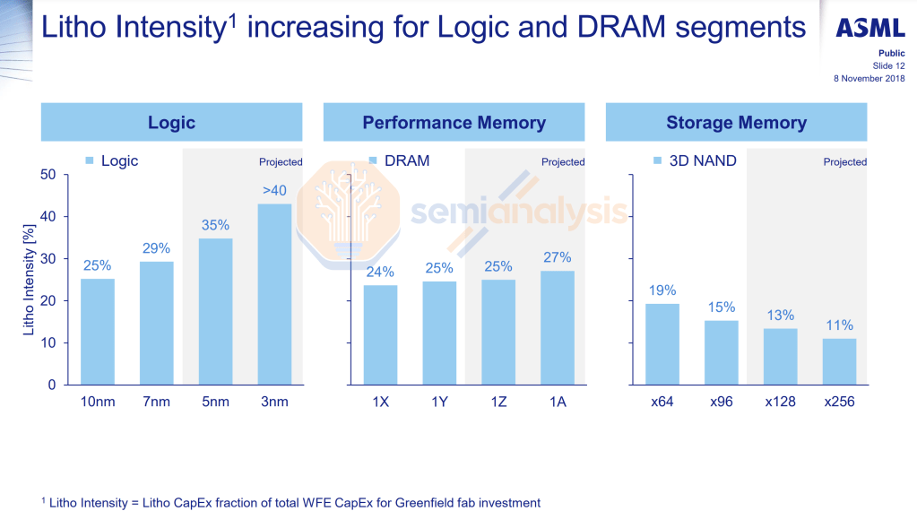
Our first example of a semicap firm being wrong on technology details will be with the largest of the bunch, ASML. ASML has consistently overstated the capital expenditure share of lithography relative to other types of tools. Here is a slide depicting lithography capex intensity associated to greenfield fabs.
This is verifiably false. Just compare the revenue from the largest semiconductor capital equipment firms, ASML, Applied Materials, Lam Research, KLA, Tokyo Electron, and ASM International.
ASML has above 95% share in lithography steppers. Our estimates put front end lithography tools at ~22% share of total front end wafer fabrication equipment sales. Most current and future capex projects are logic or DRAM, not 3D NAND, as shown in the fab tracking spreadsheet we shared below. If ASML lithography intensity estimate were accurate, the total spend share for litho tools would be closer to 30% as that’s what the blended average of capex by trailing edge logic vs leading edge logic vs DRAM vs NAND would require based on ASML’s intensity figures.
ASML has also gotten density numbers for various process nodes completely wrong. For example, this slide was presented at their investor day, 2022 SPIE Lithography and Patterning, and a few other recent conferences.
The historical density figures of 16nm, 10nm, and 7nm line up with TSMC process nodes. The 5nm figures are way too aggressive whether you use TSMC N5, Samsung 4nm, or even Intel’s unreleased 4nm. TSMC 5 is at 137.6 million transistors per mm2. Furthermore, the 3nm and 2nm estimates ASML provides are nowhere near accurate either. TSMC N3 will be closer to ~200 MTr/mm2, not 300 MTr/mm2 as shown. TSMC N2 is at most 20% more dense on maximum logic density versus N3 as per TSMC. Despite this, ASML has figure for future nodes wrong as well as those for nodes shipping 2 years ago since 2020. This slide doesn’t line up with any of IMEC, Intel, Samsung or TSMC’s claims on density.
ASML also consistently is overstating the throughput of their lithography tools. This is because they misrepresent the dose (think amount of time spent the EUV tool exposes the wafer). Their claims often assume the does is 20mj/cm2, but fabs tend to use higher. In fact, we have heard Samsung even uses as high as 60mj/cm2 in production, and most research papers similarly use that high of a dose as well. This level of dose would lead to much lower throughput figures.
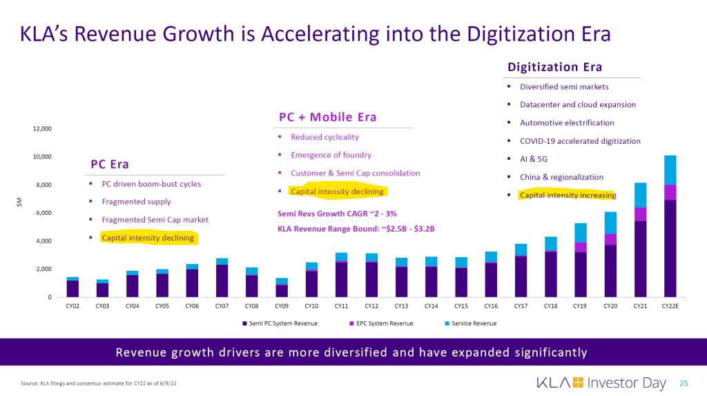
KLA is consistently the most technologically inaccurate firm in our view. To give you a taste, they made claims at their recent investor day about cost per transistor scaling, volume, and design count at each process node.
First let’s talk cost. KLA claimed that the annual reduction in cost per transistor was 22% from 2004 to 2010. They said that this cost decrease paused from 20nm to 10nm and that the industry returned back to scaling with a 23% decrease in cost per transistor since then. We could nitpick their chart on how 16nm provide cost reductions per transistor, or how 7nm+ was only ever shipped by a single Huawei chip and a single cryptocurrency mining ASIC, but let’s leave that out.
Instead, lets focus on the core claims of cost per transistor in recent history. We will use Apple chips for chip density and cost estimates as they are the highest volume chips, the first to introduce new process technologies, and achieve the highest densities on each node. In 2017, Apple released the A11 SoC with the TSMC N10 node. Last year, Apple released A15 with the N5P node. If KLA’s claims were true, we would see cost per wafer line up as below.
That would imply that the wafer cost for Apple would be well below 10,000 on N5P. Everyone and their mom like to estimate wafer costs, but I think will all agree N5P costs well above the figures KLA is implying. Furthermore, TSMC’s 5nm class nodes are still the most advanced nodes this year. They received some price hikes. Cost per transistor has certainly fallen, but very slowly.
KLA even disagreed with themselves later in their presentation. They specifically claimed that semiconductor capital intensity increasing.
KLA in this same presentation, also had some nonsense on design starts and wafers per month 3 years after a process node is introduced. This data is also verifiably false.
10nm was a short-lived node for both TSMC and Samsung. It was shipped in high volume consumer applications such as the iPhone in 2017. KLA claims that 10nm was as large as 16nm 3 years after introduction. Yet according to TSMC herself, 10nm 3 years after introduction basically doesn’t exist. TSMC 10nm was ramped down very quickly as that capacity was converted to (non-EUV) 7nm. The few leading mobile customers on 10nm moved on to 7nm after a year for their flagship SoC’s
Given 16nm is a long term node while 10nm was basically only used for a few mobile SoC’s it’s clear 16nm had a lot more designs wins than 10nm. I seriously don’t understand how KLA can get this so wrong.
The last example will be with Tokyo Electron. We love Tokyo Electron presentations as they generally share the most technical details. They also happen to get the most technical details correct. Interestingly, they happened to get this industry level financial details wrong. This could be due to them being less optimized for finance. For example, they lag behind Lam Research and Applied Materials in free cash flow conversion rates. Perhaps the flaw in their recent disclosure is due to the culture difference.
On this slide, there isn´t an axis, but magnitude the numbers can be compared. While we don’t agree with the exact numbers, generally, DRAM and NAND are directionally correct. Capex is up almost as much as density on DRAM which leads to tepid cost decreases per bit of DRAM. Capex up a lot less than the density increase on NAND which leads to a much faster cost decrease per bit of NAND.
The area we disagree with this slide is on the magnitude of increase for logic. The weirdest part about it is that TSMC announced how much they intend to spend on their gigafabs (100k WSPM) for a number of phases on Fab 20 in Hsinchu, Fab 18 in Tainan. Semiconductor capital intensity is up. Even if it were flat, the wafer costs from 7nm to 5nm to 3nm are telegraphed quite well. This means the cost for building the next technology generation gigafab is up a lot more than they described.
One could argue you should account for TSMC’s margin expansion, but that just means the cost to build the next node’s gigafab is even larger. As the cost per wafer is mostly comprised of by the total cost of tools and depreciation associated to them, the capital equipment required for the next node is clearly up significantly. In comparison to tool cost, power, consumables such as chemicals and raw substrates used by those tools, and human capital are quite low. The number of process steps from 5nm to 3nm is up ~35% to ~45%. That is a large increase in number of tools required.
To cut it short, Tokyo Electron is underestimating capital intensity increases on future process nodes. Perhaps they are just being conservative.
In the subscriber only section, we will discuss the semiconductor capital equipment companies order visibility, and we are sharing the RedFire excel file which includes details of 106 total new fabrication facilities or large expansions of existing facilities within the semiconductor supply chain. We have 61 fabs, 10 advanced packaging facilities, 13 assembly/test facilities, 7 R&D centers, and 13 wafer substrate plants tracked. Most of these sites have capex size figures associated with them. We also have the historical capex of 44 public firms with 42 on a quarterly basis.


