Cerebras Wafer Scale Hardware Crushes High Performance Computing Workloads Including Machine Learning And Beyond
Cerebras Systems and their wafer scale hardware have generated industry fan fare due to their completely unconventional approach. Rather than building a big chip dedicated to machine learning like all the other players in AI, they targeted a completely different avenue of scaling. They pursued the strategy of making the entire wafer a single chip. This hardware has shown to be surprisingly versatile and is even creating groundbreaking gains in other high performance computing applications.
This was driven by a simple observation that Moore’s law has slowed significantly. The only avenue to get huge increases in transistors count is by increasing the amount of silicon in each chip. Cerebras is on their second-generation product with the Cerebras WSE-2. This chip is has dimensions of 215mm x 215mm.
Compared to the Nvidia A100, the largest GPU available, Cerebras achieves huge advantages, especially when comparing the on chip 40GB of memory bandwidth to the A100’s similarly sized HBM memory. Cerebras has an incredibly high fabric bandwidth that far outpaces the GPU to GPU interconnects as well.
Cerebras tames their 20KW beast by offering it in a water-cooled chassis. For reference, an Nvidia A100 ranges from 250W to 500W depending on the configuration. A lot of special care had to be placed into creating this cooling solution. Issues such as differential thermal expansion of silicon and other components became a major issue due to the size and power consumption of this chip.
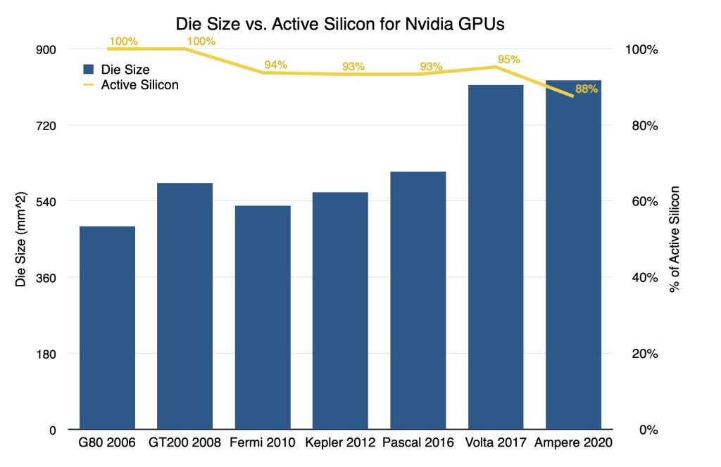
Semiconductor manufacturing has limited die size has been limited by the reticle limit for a long time. The reticle limit is 33x26 meaning that this is the largest size a lithography immersion stepper from ASML can pattern on a wafer. Nvidia’s largest chips are in the low 800mm^2 range mostly because going beyond this is impossible.
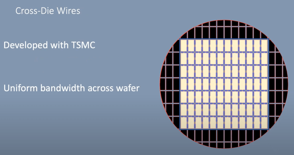
The Cerebras WSE is actually many chips on a wafer within the confines of the reticle limit. Instead of cutting the chips apart along the scribe lines between chips, they developed a method for cross die wires. These wires are patterned separately from the actual chips and allow the chips to connect to each other. In effect, the chip can scale beyond the reticle limits.
When building chips in a classical way, there are often defects. As such, a number of chips from each wafer must be thrown away or elements of a chip must be disabled. Nvidia commonly uses this practice with their GPUs. There has been an ongoing trend of disabling a larger percentage of cores with each new generation and with their current generation Ampere, roughly 12% of cores are disabled.
Cerebras deals with this by adding 2 additional rows of cores across each reticle sub-chip. The interconnect within these chips is a 2D mesh where each core is connected in the vertical and horizontal directions. They also have additional interconnects for each of the diagonal cores as well. This allows defective cores to be routed around and software to still recognize a 2D mesh.
Within this 2D mesh, Cerebras targets a few goals. They wanted all memory to remain on chip rather than having to wait for slow off chip memory. The only external connection is to the host system. Each core has fine grained parallelism and shares nothing between each other. They are power efficient and general-purpose cores capable of MIMD and have their own local memory.
The primary use case is for machine learning training or inference. Layers of networks are mapped to regions of the wafer sized chip. Each rectangular block corresponds to a layer and is interestingly called a “Colorado.” Convolutions, matrix vectors, and matrix multiplications are computed on cores within each layer. The 2D mesh handles inter core communications within each layer of the network and in between layers of the network.
Most communications are generally in either X or Y along the chip, but some communications need to cross huge portions of the chip. The mesh can handle this without getting congested. This allows layers within a network to not have to be contiguous or directly next to each other. Cerebras software stack places and routes these layers while maintain high utilization rates of cores and fabric. The software is capable of placing only a few layers of a network on a single chip or placing multiple copies of the entire network across the chip for data parallelism.
Cerebras has customers with live production wafer scale engines. These are used in many different workloads, but one of the most interesting is CANDLE. The WSE is used for precise simulations of drug response for combinations of drugs and their effects on cancer. The most promising results from simulations are then selected for experimental investigation.
Another current use case running on these chips is for internal confinement fusion. This runs on a large supercomputer that also contains multiple interconnected Cerebras WSEs. One of the components in this massive simulation involves interactions between atoms and sub-atomic particles. This computation is replaced with a large pre-trained neural network that runs on Cerebras hardware. This is a use case where only inference is used. It is evoked at every time step of the simulation. Data is streamed from the larger supercomputer to the Cerebras WSEs which in turn provide the output for these atomic and sub-atomic interactions.
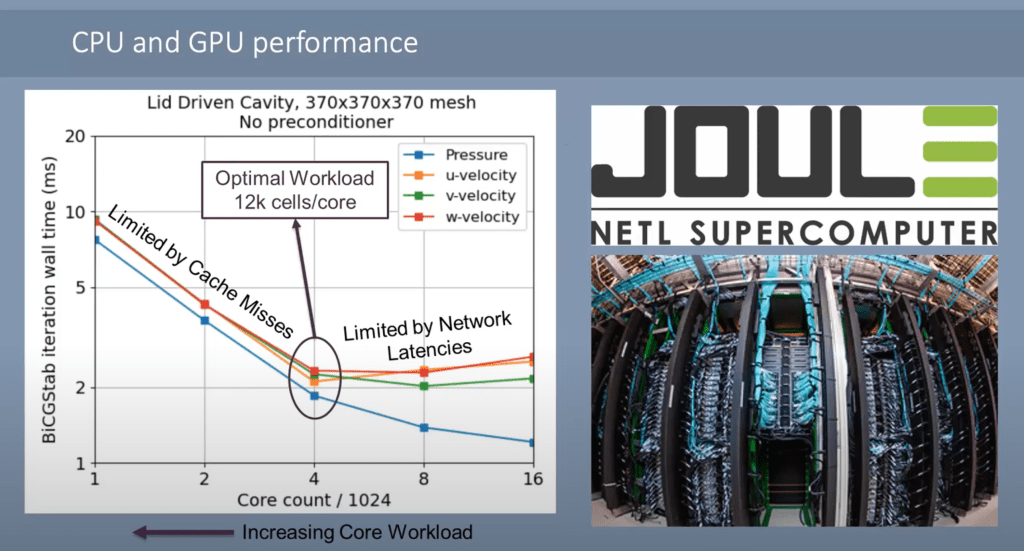
Cerebras hardware is used beyond just machine learning too. The Joule supercomputer runs computational fluid dynamics on conventional hardware running in a 3D mesh. They have run into a scaling problem in two different ways. They could not scale up performance with core counts due limitations in network bandwidth. Furthermore, the cores were often leaving a lot of performance on the table due to cache misses and therefore going out to memory. This memory then ran into huge bandwidth bottlenecks.
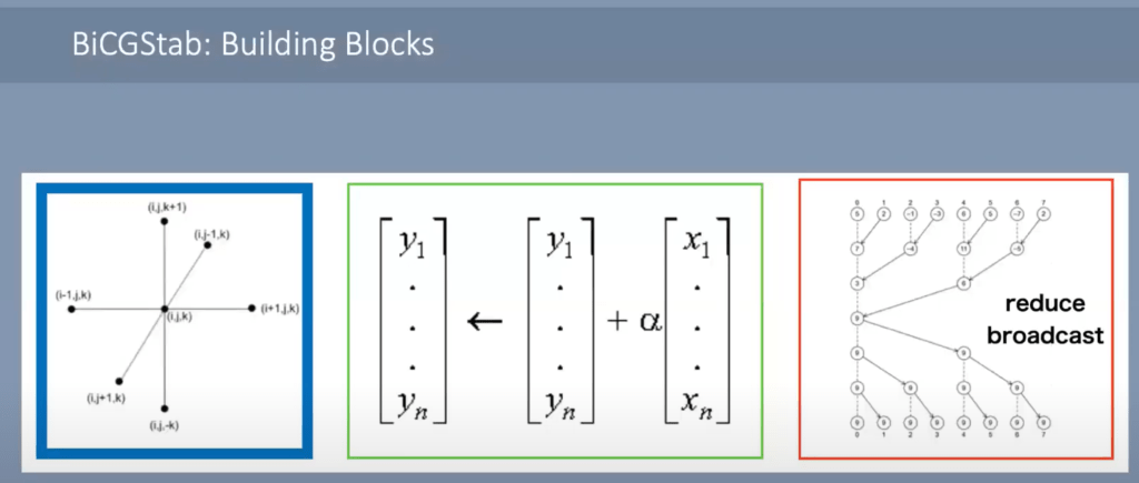
The 3D mesh of the fluid dynamics model was mapped to the 2D mesh of the WSE chip. Neighbor exchange, vector AXPY, and dot products of global vectors which entails local dot products and a global all-reduce. All these operations can be handled with ease due to the large amount of SRAM and relatively high complexity of each individual core.
There is a large amount of inter-core communications, but the internal network on chip is robust enough to handle them with low latency. The network does this by sending messages along virtual channels called “colors” rather than to pre-determined addresses. This hardware-based communications allows data to travel 1 hop per clock across the entire chip.
Allreduce can be done incredibly fast. Each core sends its scalar to the core next to it. When it arrives there, the scalars are added together and sent forward. The edges of the chips are sending data east/west towards the center. Once it arrives in the center, the same process occurs but north/south. The results are coalesced and then broadcasted back over the mesh of cores. In just 1 microsecond, this allreduce can be completed. For reference, a typical cluster in a supercomputer takes about this long for a single MPI communication from 1 processor to another neighboring processor.
Computations can be done to achieve full bandwidth regardless of delays to bringing data in. The router has 4 incoming sets of data from each adjacent core. In addition, the core can reroute its output back in so that it does not need to be store it in SRAM. The core can run multiple threads at once. There is a main thread that is given priority, but if it is waiting on data, the other threads will progress. By maintaining data locality with large amounts of SRAM and a multithreaded architecture, utilization rates are kept extremely high.
The results of the low-level optimizations to the hardware resulted in a 200x speed increase in computational fluid dynamics. This is in comparison to a large supercomputer cluster which was also highly optimized. In addition to the speed up, cost and especially power had tremendous advantages. This advantage is somewhat obvious as a supercomputer cluster is being compared to a single, albeit wafer sized, chip.
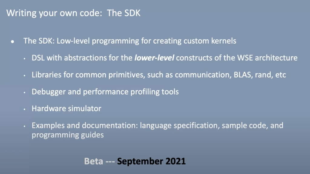
Unfortunately, software is not completely up to snuff yet. A beta SDK will come later this year for writing custom kernel operations. This language would be completely domain specific to the WSE. They will have libraries for mathematical functions and communications which should hopefully lift the burden somewhat. Beyond this, there are some features and tools that will help, but it will be a high skill programmers’ task. This is the only hardware that can achieve this scale of computing, so it may not be a massive barrier to entry for those tasks that require this level of performance.
Cerebras is pitching real time computational fluid dynamics as the next workload to take advantage of WSEs. There is considerable promise that this will open a completely new use case.
We are excited for the 7nm based WSE2 to roll out fully. It will be exciting to see if the SDK can allow developers to generate other workloads where the WSEs can bring orders of magnitude performance increases. AI is an area where Cerebras is being aggressive and turning heads, but wafer scale computing could change this industry far outside of just machine learning.
This article was originally published on SemiAnalysis on June 30th 2021.
Clients and employees of SemiAnalysis may hold positions in companies referenced in this article.


