CXL Is Dead In The AI Era
AI Accelerator Beachfront Considerations, Memory Pooling Negatives, Custom Silicon Adoption
If we travel back 2 years in time, before the rapid rise in AI, much of the datacenter hardware world was chasing CXL. It was promised as the messiah to bring heterogenous compute, memory pooling, and composable server architectures. Existing players and a whole new host of startups were rushing to integrate CXL into their products, or create new CXL based products such as memory expanders, poolers, and switches. Fast forward to 2023 and early 2024, and many projects have been quietly shelved and many of the hyperscalers and large semiconductor companies have almost entirely pivoted away.
With the upcoming Astera Labs IPO and product launches, CXL discussions are coming back to the front row at least for a short while. We have written extensively about the technology, its cost savings potential for Cloud Service Providers, and the ecosystem & hardware stack. While very promising on paper, the datacenter landscape has evolved a lot, but one thing hasn’t changed: CXL hardware such as controllers and switches are still not shipping in meaningful volumes. Despite this, there is still a lot of noise and research around CXL, with certain professionals in the industry now pushing the narrative of CXL as an 'enabler' of AI.
Is the broader CXL market ready to take off and deliver on its promise? Can CXL become the interconnect for AI applications? What is the role in CPU attach expansion and pooling? We will answer these questions in the subscriber section of this report.
The simple answer is no - the people pushing CXL for AI are dead wrong. Let’s start with a quick reminder of the main use cases and promises of CXL.
Quick CXL Refresher Overview
CXL is a protocol built on top of the PCIe physical layer, enabling cache and memory coherency across devices. Leveraging the wide availability of PCIe interfaces, CXL allows memory to be shared across various kinds of hardware: CPUs, NICs & DPUs, GPUs & other accelerators, SSDs, and Memory devices.
This enables the following use cases:
Memory expansion: CXL can help increase memory bandwidth and capacity for servers.
Memory pooling: CXL can create memory pools where memory is disaggregated from the CPU, which, in theory, could massively increase DRAM utilization rates. On paper, this could save billions for each Cloud Service Providers.
Heterogenous compute: ASIC’s are far more efficient than general purpose CPUs. CXL can help enable heterogenous compute by providing a low latency cache coherent interconnect between ASIC’s and general purpose compute so applications can integrate them into existing code bases more easily.
Composable server architectures: Servers are broken apart into their various components and placed in groups where these resources can be dynamically assigned to workloads on the fly, improving resource stranding and utilization rates while also better matching application needs.
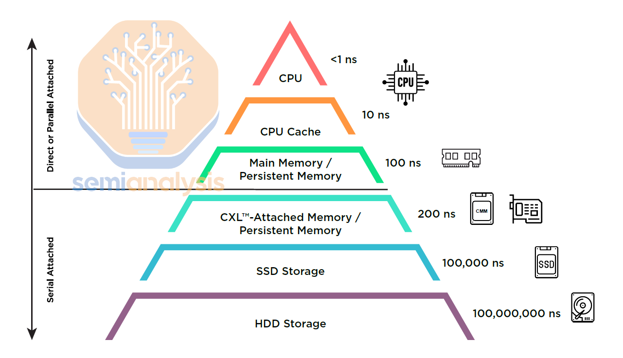
The below figure tells part of the story: CXL could solve the latency and bandwidth gaps between main system memory, and storage, to enable a new memory tier.
Some folks are now forecasting CXL sales of up to $15 billion by 2028 versus a few millions today, so we felt it was time for a proper update on the CXL market, because that is an outright ridiculous claim. Let’s start by addressing the case of CXL for Artificial Intelligence.
CXL Will Not Be The Interconnect of The AI Era
Currently, CXL availability is the main issue, as Nvidia GPUs don't support it, and with AMD the technology is limited to the MI300A. While the MI300X can theoretically support CXL in hardware, it is not exposed properly. Availability of CXL IP will improve in the future, but there exist deeper issues than just availability that render CXL irrelevant in the era of accelerated computing.
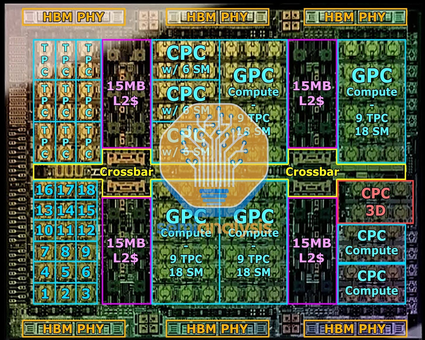
The two main issues are related to PCIe SerDes and beachfront or shoreline area. IO for chips generally must come from the edges of the chip. The below picture from Nvidia shows the H100 in a cartoonized format. The center has all the compute. The top and and bottom sides are 100% dedicated to HBM. As we move forward from the H100 to B100, the number of HBM grows to 8, requiring even more shore line area on it. Nvidia continues to consume two entire sides of their 2 die package with HBM.
The remaining two sides are dedicated to other chip to chip IO, and this is where standards and proprietary interconnects compete for die area. A H100 GPU has 3 IO formats: PCIe, NVlink, and C2C (for connecting to Grace). Nvidia has decided to include only the minimum 16 PCIe lanes, as Nvidia largely prefers the latter NVLink and C2C. Note that server CPUs, such as AMD’s Genoa, go up to 128 lanes of PCIe.
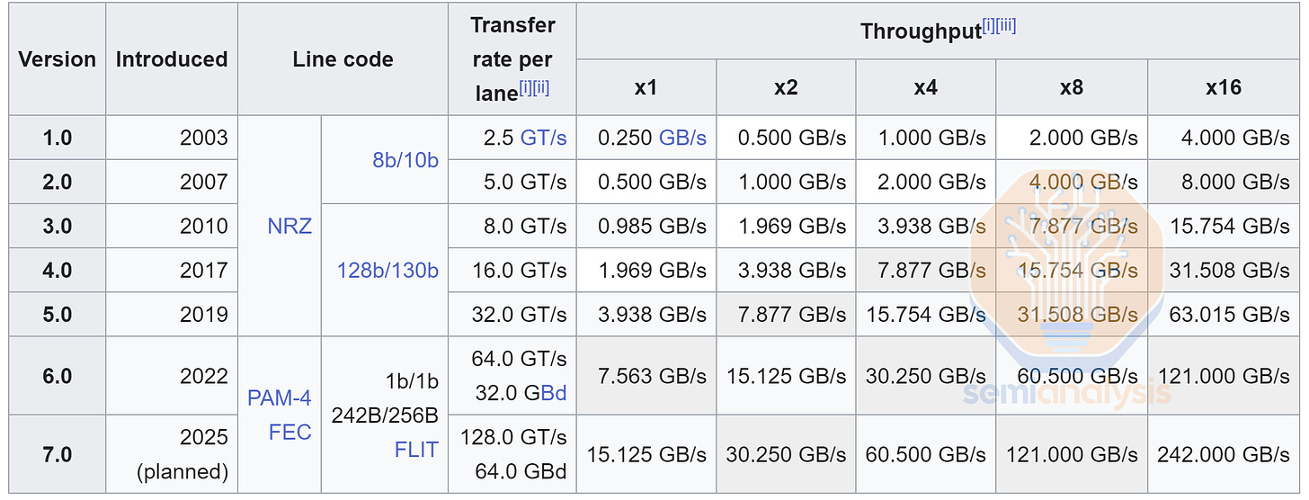
The main reason for this choice is bandwidth. A 16-lane PCIe interface has 64GB/s of bandwidth in each direction. Nvidia’s NVlink brings 450 GB/s bandwidth in each direction to other GPUs, roughly 7x higher. Nvidia’s C2C also brings 450GB/s bandwidth in each direction with the Grace CPU. To be fair, Nvidia dedicates far more beachfront area to NVLink, we so need to include silicon area in that equation; but even so, we estimate that per mm² across a large variety of SOCs, Ethernet-style SerDes such as Nvidia NVLink, Google ICI, etc have 3x more bandwidth per unit of shoreline area.
Therefore, if you are a chip designer in a bandwidth constrained world, you are making your chip roughly 3x worse when you chose to go with PCIe 5.0 instead of 112G Ethernet-style SerDes. This gap remains with next generation GPUs and AI accelerators adopting 224G SerDes, keeping this 3x gap with PCIe 6.0 / CXL 3.0. We are in a pad limited world, and throwing away IO efficiency is an insane tradeoff.
The main scale up and scale out interconnects for AI Clusters will be proprietary protocols such as Nvidia NVlink and Google ICI, or Ethernet and Infiniband. This is due to intrinsic PCIe SerDes limitations even in scale up formats. Due to diverging latency goals, PCIe and Ethernet SerDes have dramatically different bit-error-rate (BER) requirements.
PCIe 6 requires a BER of < 1e-12 while Ethernet requires 1e-4. This massive 8 orders of magnitude difference is due to PCIe's strict latency requirements, necessitating an extremely light forward error correction (FEC) scheme. FECs digitally add redundant parity bits/information at the transmitter which is used by the receiver to detect and correct errors (bit flips) much like ECC in memory systems. Heavier FECs add more overhead, occupying space that could be used for data bits instead. More importantly, FECs add a large amount of latency on the receiver. This is why PCIe has avoided having any FEC up until Gen6.
Ethernet-style SerDes are much less constrained by stringent PCIe specifications, allowing it to be much faster and have higher bandwidth. As a result, NVlink has higher latency, but this doesn’t matter as much in the AI world of massively parallel workloads, where ~100ns vs ~30ns is not a worthy consideration.
First off, the MI300 AID uses most of its beachfront area for PCIe SerDes instead of Ethernet-style SerDes. While this gives AMD more configurability in terms of IFIS, CXL, and PCIe connectivity, it results in the total IO being about 1/3 that of Ethernet-style SerDes. AMD needs to immediately move off PCIe-style SerDes for their AI accelerator if they want to have any hopes at competing with Nvidia’s B100. We believe they will be for MI400.
Nvidia’s Plans To Crush Competition – B100, “X100”, H200, 224G SerDes, OCS, CPO, PCIe 7.0, HBM3E
AMD’s lack of high quality SerDes are severely limiting them in the competitiveness of their products long term. They have come up with the Open xGMI / Open Infinity Fabric / Accelerated Fabric Link, because CXL is not the correct protocol for AI. While it is primarily based on PCIe, it does eschew some of the standard features of PCIe 7.0 and CXL for time to market, performance, coherence, and reach reasons.
What about CXL memory bandwidth expansion for AI? What about the custom AI hyperscaler chips adoption? What about the other custom silicon chips from other vendors such as the Marvell Google CXL chip? We will address those questions and review the more classic Memory Pooling and Memory Expansion use-cases.


