Embracing Chaos: The Imperfect Art of Semiconductor Manufacturing And Lithography
5 Longs, Intel EUV Delayed Again, And More
All manufacturing in the world is built upon stacking multiple processes and systems with various tolerances and variation ranges to get a consistently useful product. Nowhere is this more evident than in semiconductor manufacturing due to being the single most complicated manufacturing process with the lowest tolerance for error in the world. Despite these challenges, the semiconductor industry has stacked hundreds of abstraction layers on top of each other for the software world to see a consistent device. As the layers are peeled back, an extreme amount of variation reveals itself.
Each chip that comes out of a fab, even if it is the same design, consumes a different amount of power for any given level of performance. Many chips will have defects that lead to the final chip being yield harvested with several disabled “cores” and IO. For example, all Nvidia A100 and H100 GPUs ship with ~10% of the chip disabled. The reason is the manufacturing variations embedded within the billions of transistors and interconnects on modern high-performance semiconductors, created with thousands of different process steps. Each individual transistor will take a different amount of voltage to switch. Each section of interconnect, via, and contact will have different resistance.
Let’s look at EUV lithography, as this is one of the technologies central to manufacturing advanced semiconductors. Our readers probably don’t need a crash course on lithography, but if you do, see these posts. 1, 2, 3, 4, 5, 6, 7. From the source of EUV light to the mirror system to the photomask to the alignment system to the wafer stage to the photoresist chemical composition to the coater and developer to metrology to the individual wafers.
EUV is a process fraught with complexity, uncertainty, and imperfection, yet it works. TSMC, Samsung, and SK Hynix are all in production of EUV at varying volumes. Intel has also confidentially stated that they are manufacturing ready for EUV lithography in their Intel 4 process node. We don’t really believe them because internal documents we obtained show Intel’s first high-volume product utilizing EUV, Meteor Lake, has been delayed yet again, with “ready-to-ship” dates delayed until Week 52, 2023 at minimum. This suggests that Intel is facing challenges in implementing a production-scale design into an EUV process technology.
The accumulation of slight variations in individual process steps can add up to a significant deviation from the desired outcome, ultimately leading to the failure of the final product. For example, issues with laser drilling or precision casting in aircraft engines could lead to a turbine blade being unbalanced. This unbalanced turbine will cause additional vibration, reducing efficiency and eventually leading to the engine wearing out and failing earlier. Now consider that aircraft engines are significantly simpler than semiconductors in manufacturing precision, process variation tolerance ranges, chemistry, physics, and number of steps.
Most tools in a leading-edge fab can deposit, polish, or etch materials within the precision of a handful of atoms. Each subsequent tool in the chain of thousands of tools/process steps will constantly have its process parameters tweaked. These conditions and tweaks are determined by utilizing process control. Process control includes metrology/inspection tools and the software which controls it. Fabs spend more than $20 billion annually on process control.
If an etch tool has four chambers, process control intelligence, and fab network routing will determine which of the four chambers to send wafers to based on availability and yield metrics in that process step. They will also adjust the chamber conditions and monitor if maintenance is required. In fact, even trailing edge fabs will tweak tool settings for each individual wafer or lot to keep the accumulated tolerance range for each feature to a minimum viable specification.
To emphasize this point, the high level of variation and uncertainty is so pervasive that production fabs will test a photomask with multiple different EUV tools. These production fabs may run that photomask on only one specific EUV tool that produces the highest yield or most manageable defects. Note that a modern TSMC 5nm design has ~81 masks, and a single fab will run dozens or hundreds of designs a year. Furthermore, photomask to EUV tool matching is retested regularly as masks must be serviced or remade on a semi-regular basis.
Similarly, even when metrology/inspection tools of the same type are created and shipped from the same facility, they may only be used on select layers due to the high level of tool-to-tool variation when measuring features that are only a few atoms in size. In fact, in some cases, more than 25% of the error budget (stacked variations) is consumed by the uncertainty of the metrology and inspection imaging tools. The tools designed to provide the data to help adjust the tools and processes in flight are also so imperfect that it’s like trying to fly at night.
Fabs have to jump through many, many holes to even trust that their metrology equipment is giving them an accurate picture of what’s actually happening on the wafers they are processing. Many of the errors and defects stem from EUV tools and processes. EUV has 1/14th of the photons hitting the wafer relative to DUV at the same dosage. As such, this introduces a considerable number of stochastic defects stemming from a more random distribution of fewer photons. Stochastics in EUV lithography refers to the random variations that can occur in a pattern.
These stochastic defects are a multi-billion dollar problem for the wafer fabrication industry. Tens of billions of dollars are spent characterizing variation with metrology and inspection tools. The data generated here is then fed back into the modifying process or tool parameters on a wafer-by-wafer, design-by-design, or tool-by-tool perspective. No two wafers, tools, or designs are alike, and there is a tremendous amount of adjustment and optimization on each of these fronts in a fab network.
A gigafab will run 1000’s steps across ~250,000 in-flight wafers, with ~100,000 finishing over a month and a new 100,000 starting over a month. The logistical challenges of routing, optimization, and making decisions cannot be understated.
Stochastics are not just growing linearly, but they're growing exponentially as a percentage of the critical dimensions that we are printing.
Chris Mack
We had the chance to chat with Chris Mack, aka the “Litho Guru,” about many of these difficulties that the industry faces and some of the solutions that have been developed. For those of you who don’t know, Chris Mack famously bet a Lotus Elise that EUV wouldn’t be ready by a specific date at the SPIE Lithography and Advanced Patterning conference. Another funny story is that he made and wore a red “Make EUV Great Again” hat at this conference as a joke.
The SPIE Lithography and Advanced Patterning conference is this week. We regularly attend it as it covers all the latest developments in the photoresist, photomask, metrology, inspection, and lithography. If you’re at SPIE Lithography and Patterning this week, let us know, and we can chat!
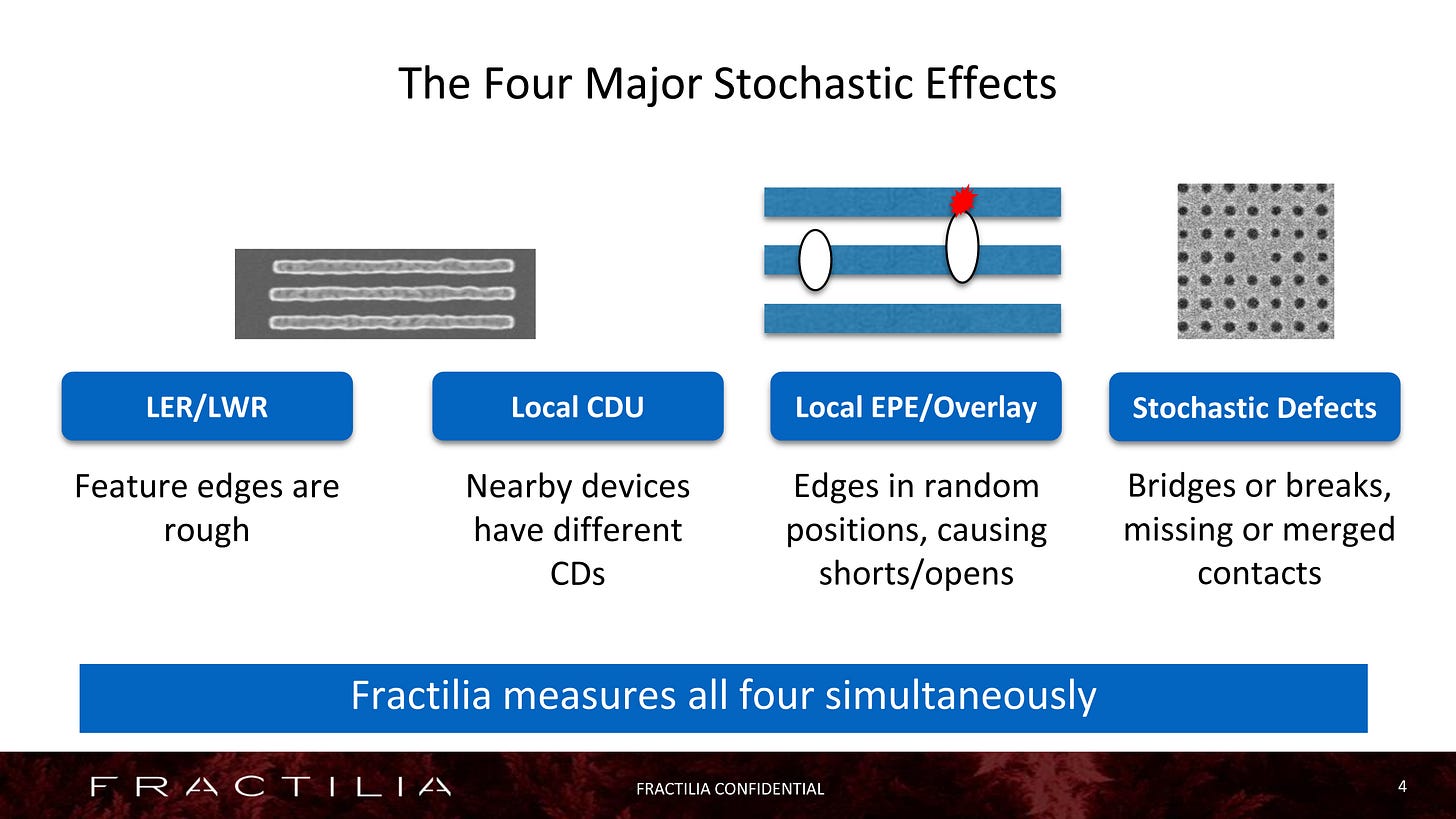
There are a handful of major classes of variations and defects. These can all increase wire resistance, the leakage of a gate, or even cause shorts or other defects that render a chip unusable.
Overlay / Local Edge Placement Error
As mentioned earlier, a TSMC 5nm process has ~81 photomasks. This is 81 different instances of going through the entire lithography process. In addition, there will be thousands of other manufacturing steps in between.
Overlay or local edge placement error is the variation of placement of one feature from a deposition, lithography, etch cycle on top of another feature from a prior cycle. A +1nm misalignment on one layer and a -1nm misalignment on the next layer stacks up to a 2nm difference in the placement of a feature. These sorts of errors can stack up cumulatively over many steps and can be catastrophic.
One example we have discussed here is self-aligned contacts at TSMC vs. Intel, which attempt to mitigate some of the stacking of overlay errors by making the patterned features more resistant to placement errors.
Local Critical Dimension Uniformity (CDU)
Another major source of variation is local critical dimension uniformity. Features next to each other should ideally be uniform if we want them to be, but in many cases, they are not. In this example, let’s zoom out to the vias and contacts that connect various metal layers of chips.
When these stochastic variations get large enough, they result in defects missing or merged: contact poles, bridges, and breaks and lines and spaces. And if you have 100 billion contacts/vias on a chip and one of them goes missing, your whole chip is dead (some redundancy will be built in, of course). The industry must have at about one in 100 billion defect rates for features that are only tens of nanometers in diameter.
Line Edge Roughness (LER)
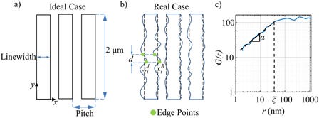
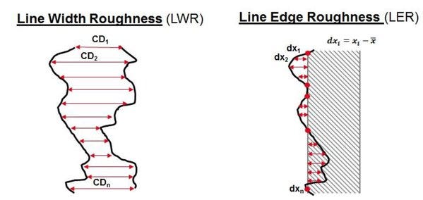
Line edge roughness (LER) is a variation in the edges of features. LER can be defined as the roughness or irregularities in the edges of patterned features, such as lines or trenches, which can lead to deviations from the desired critical dimensions.
LER can have a significant impact on the performance and reliability of the final product. For example, in the case of transistor gates, variations in LER can affect the transistor's electrical properties, leading to issues such as increased leakage currents and reduced device performance.
Line Width Roughness (LWR)
LWR can be defined as the roughness or irregularities in the width of features, such as lines or trenches, which can lead to deviations from the desired critical dimensions. In the case of metal interconnects, variations in LWR can affect the resistance of the lines, leading to issues such as increased power consumption or reduced device performance.
Optical Proximity Correction (OPC)
The photomask can be thought of as the stencil of a chip. A photomask is patterned with ebeam and placed inside the lithography tool. The photomask can then absorb or scatter the photons or allow them to pass through to the wafer. This is what creates the pattern on the wafer.
OPC aims to correct distortion or deformation of patterned features that occur during the lithography process. By compensating for them, manufacturers can achieve higher accuracy and consistency in the patterned features, leading to improved performance and reliability of the final product. Below is an early form of OPC with more advanced conditions, including using curvilinear ILT masks in volume at TSMC.
We also will share five public firms that could have outsized benefits from the chaos of lithography and art process control. None of them are ASML or KLAC if that’s what you were guessing.


