EUV Requirements Halved? Applied Materials' Sculpta Redefines Lithography And Patterning Market
$4.5B EUV Annual Reduction, High-NA, Contacts, Vias, Throughput, ASP, Use cases, TSMC N2, Intel 18A, Samsung 2nm
ASML’s EUV lithography tools are expensive... Really expensive. Each EUV tool is now approaching $170M, and you use many of them for a leading-edge semiconductor fab. In the future, the cost of each High-NA EUV tool will be in excess of $350M. In addition, you need many DUV lithography tools for these fabs as well. Everyone wants a more cost-effective way to pattern chips given lithography alone consumes ~35% of the cost of a 3nm process node. Imagine if there was a way to break this trend…
Last week, Applied Materials, the 2nd largest semiconductor equipment manufacturer in the world, announced they have a potential solution. That solution is the Centura Sculpta tool, a new tool that can perform a new process step, “pattern shaping”. According to Applied Materials, the Sculpta tool could be used to reduce the use of EUV lithography by as much as HALF for some layers. If true, this would reshape the cost structure of the industry. There’s a lot of room to be skeptical of Applied Material’s claims, so let’s bring on the nuance for this discussion.
This report will be a deep dive into the new Centura Sculpta. We will discuss how the technology works, the impact on EUV multi-patterning and High-NA EUV, where it could be used (front end, contacts, vias, various metal layers, dose reduction), and how these use cases could evolve with future process technology scaling. Furthermore, this report will contain a cost comparison for a real process node using EUV or a mix of EUV and Scuplta. We will share the tool’s throughput, cycle time, cost, our shipment estimates, and revenue estimates from the first customer.
We will share how we arrived at a potential $4.5 billion dollar reduction in EUV demand, what year the impact would be that size, and what could move that figure up/down. We will directly discuss TSMC, Samsung, and Intel’s adoption and insertion points for Centura Sculpta with 2nm class nodes. This will include specific process node details including minimum pitch and Sculpta layers for an upcoming process technology that will use Applied Material’s Sculpta. The pros and cons of this decision will be discussed.
We will discuss the impact on other process steps including lithography, photoresist, coater/developers, CVD, PVD, etch, CMP, epitaxial growth, ion implantation, metrology, and inspection from the introduction of a new pattern shaping step. Pattern shaping has many ramifications for suppliers in the industry including but not limited to ASML, Lam Research, Tokyo Electron, JSR, TOK, Shin-Etsu, Lasertec, KLA, Onto, Nova, Hoya, and Asahi Glass.
To start with, there has been a lot of dismissal of this tool by folks in the semiconductor and finance industry, despite there being a very clear use case for it. Some argue that it isn’t anything new and it’s just a fancy expensive form of inductively coupled plasma doing a reactive ion etch which has been around for decades in high-volume manufacturing. To that, one could also argue that lithography has been around for 150 years and EUV is nothing new too. The shaping use case is clearly unique.
Another one of the primary dismissals has been that it’s immature, and very far out. That is also wrong. While Sculpta was only officially announced last week at the SPIE’s Lithography and Advanced Patterning conference, this new tool has been coming for a long time. Applied Materials has been releasing public research papers on this tool type since at least 2015. The first customer has been working with Applied Materials on the tool since ~2017. Applied Materials even had a technical presentation on it last year at the SPIE Advanced Lithography & Patterning conference with real customer test data.
A funny story about that specific presentation. After it concluded, we left the presentation room and spoke with a few of our fellow attendees. The general consensus was that it was super cool, but it wasn’t going to work. Why? Presentations from companies at SPIE fall into 3 buckets. 1, what is entering production soon, 2, what is many years away and to plant a stake in the ground, and 3, what doesn’t work at all but is being presented because there is nothing else to do with the data. The assumption we had last year was that it was #2 and/or #3. That was an incorrect assumption.
Applied Material’s Centura Sculpta is not some crazy tech that is completely immature and far away from production. Sculpta is real, it does work, and it will generate hundreds of millions of dollars in revenue over the next couple of years. Given it is being billed as directly removing EUV double patterning in the first use case, first let’s quickly review the lithography multi-patterning process.
Lithography Multi-patterning Process
Lithography is the central process in high-volume semiconductor manufacturing. We will skip past explaining the basics, but you can refer to our prior reports on the topic. 1, 2, 3, 4, 5, 6, 7
Once you go past the limits of the lithography tool, you can still keep scaling single feature sizes by moving to various multi-patterning schemes. Below is a simplified depiction of “litho-etch-litho-etch (LELE),” one of the most common multi-patterning schemes. We will bucket other schemes like SADP and LELB into the same bucket as LELE for simplicities sake here.
The LELE process flow goes through the full lithography cycle twice to achieve feature sizes tighter than what a single patterning step is capable of. The full cycle can be dozens of different process steps including deposition of hard masks, underlayers, mid-layers, BARC, CMPs, cleans, strips, spin coats, bakes, develops, exposures, etches, and various metrology/inspection steps in between.
The key point is that going from a single lithography cycle to a LELE process involves doubling your lithography costs as well as many other tools involved in the process.
Applied Materials is specifically targeting EUV multi-patterning reduction as the 1st use case for Sculpta. They claim they can achieve the same features fidelity as LELE with a single litho cycle and Sculpta.
We estimate about 25 kilowatt-hours per wafer, about 0.5 kilograms of CO2 equivalent emissions per wafer and about 15 liters of water per wafer per LE (Litho-Etch) loop. And on the right box, we show the cost. We estimate about $350 million of capital cost per 100,000 wafer starts per month and about $70 per wafer manufacturing or OpEx cost per wafer per EUV loop. The cost savings, we estimate about $250 million of capital cost per 100,000 wafer starts per month and about $50 per wafer of manufacturing costs saved.
The cost, power, water, and CO2 savings claims from Applied Materials are tremendous. TSMC has ramped their 7nm and 5nm nodes to (roughly) 200,000 wafers per month. Per layer, this would save them $500 million of CapEx and over $100 million on annual operating expenses. Our numbers differ and we will share them later.
TSMC 5nm has a EUV multi-patterning step. TSMC 3nm contains multiple EUV multi-patterning steps. This technology is targeting insertion in “2nm” class nodes, which could contain more than 10 EUV multi-patterning steps without Applied Materials Sculpta pattern shaping. The use of Sculpta could save *billions of dollars* a year if you assume that it can be used *everywhere*.
That analysis is overly simplistic and pattern shaping cannot be used everywhere. We will share where and how it can be used, but first let’s talk about what Sculpta and pattern shaping even are.
What Is Centura Sculpta and Pattern Shaping?
The core of Centura Sculpta is being able to perform a new type of step called pattern shaping. Pattern shaping is shooting a ribbon beam of plasma at the wafer at an angle. The angle can be controlled from 0 to 70 degrees compared to the wafer. The zero angle is 90 degrees from the angle of the wafer. Perpendicular.
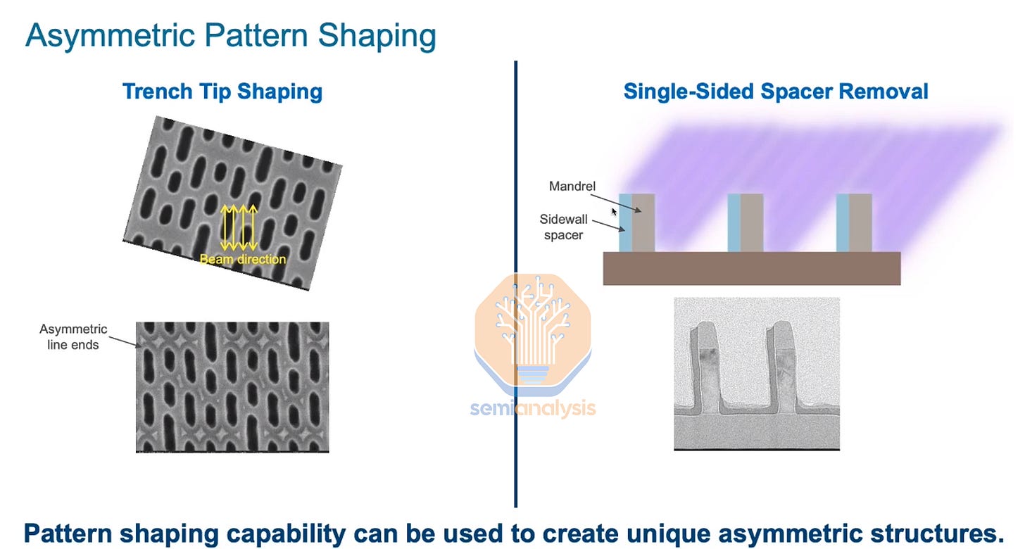
The plasma beam travels in one dimension in order to keep the processing uniform across the wafer. The purpose is unidirectional elongation of features in 1 direction. Pattern shaping can be performed in any direction by rotating the wafer around and running the beam across the wafer again.
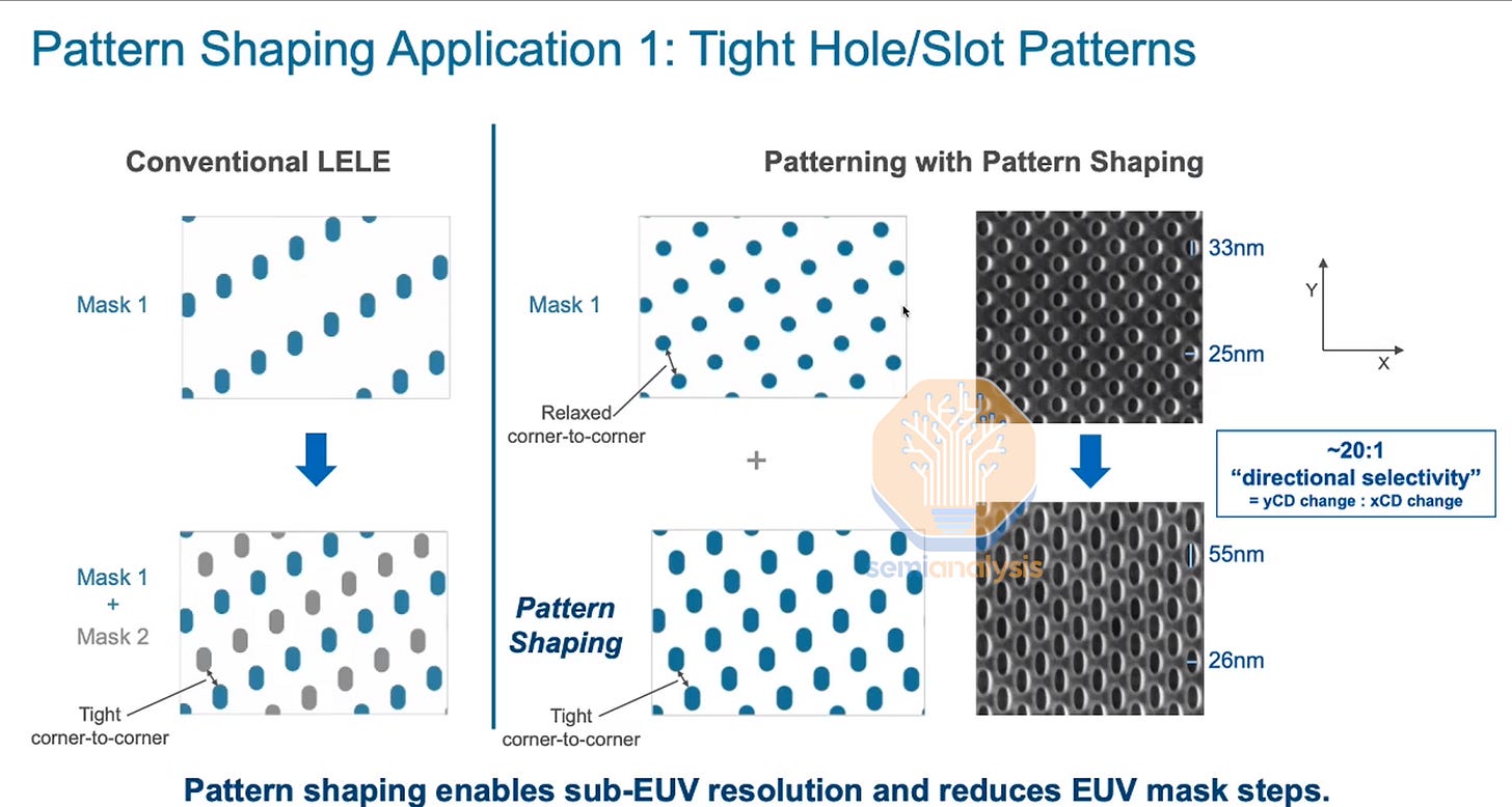
It is critical for pattern shaping to not affect the critical dimensions of the silicon features that need to stay the same. This means that only changing the feature on one axis is critical. Applied Materials says that they can change a single dimension by a factor of 20 units of length for every 1 unit of length in the other direction.
This is highly selective directionally. The fab can also control how much a pattern is elongated by increasing or reducing the time spent being bombarded by the ribbon beam. Etch time is an important lever that the fabs can play with.
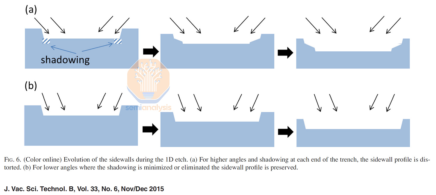
Another consideration for keeping shapes uniform is making sure that the beam angle is optimized for a variety of different structures on the wafer.
If the beam angle is incorrectly aligned, then you could have shadowing occur on structures of different sizes.
If the planarization layer and the hard mask have different etch selectivity, then the plasma beam will cause the sidewalls to not be uniformly straight.
The sidewall profile of a feature must be optimized or there will be performance, power, or yield issues.
The angling of the plasma beam is incredibly important for fabs to optimize to ensure features of various sizes will have uniform and consistent elongation amounts. Using a higher angle vs lower angle will juggle factors such as the time required to etch, the erosion rate of the top layer, and the erosion rate of the bottom layer to keep the critical dimension intact. Each application will have different beam angles and time. Applied Materials has worked on multiple different chemistries so the beam can be used with a variety of hard masks, underlayers, and midlayers.
Pattern shaping happens after the develop, clean, and etch through of the photoresist and anti-reflective coating layers.
Once the pattern shaping has occurred then the pattern transfer etch can be done. This allows pattern shaping to be used even if you have multiple masks and patterning stages. Pattern shaping can be combined with multi-patterning.
Pattern shaping doesn’t just need to be in the direction of the existing features. It can also be done at any arbitraty angle. For us, this seemed more of a showcase of Applied’s alignment and process control with the Sculpta rather than there being an actual use case of asymmetric shaping. We can’t think of a usecase for asymmetric shaping, but please do share if you think there is one.
Now that we have covered what pattern shaping is, it’s time to cover the actual use cases for pattern shaping.
Use Cases
There are 3 major use cases for the Scuplta tool: Tight hole and slot pattern, narrower tip-to-tip patterns, and removing stochastic bridging.
The first application is getting hole and slot patterning with tight corner-to-corner dimensions using traditional litho-etch (LE) methods you would require multi-patterning. With pattern shaping, you have the advantage of only needing to use only one LE step to get tight corner to corner. Tight corner-to-corner is important because it lets you be able to put more features, into the same area. In this case with vias, this gives you improved performance and power characteristics due to having more area for the vias.
In the image above, you can see on the left how a tight corner-to-corner would be accomplished using conventional self-aligned LELE techniques. You require 2 different masks for a tight corner-to-corner of the vias but with pattern shaping, you can use a single mask to create all the vias without tight corner-to-corner, then shape the vias to have a tight corner-to-corner.
The second application is producing trenches with a tighter tip-to-tip pattern. This is very similar to the first application, but with a different feature type. In this application, pattern shaping is used to get two sets of lines as close together as possible without using a second mask.
On the left is the conventional LELE technique. The first mask creates the lines then the second mask creates a split between the two to get as tight of a tip-to-tip spacing as possible. With pattern shaping, you use one mask to create the 2 sets of lines with a loose trench in the middle. Then Sculpta can remove as much material as possible to make the trench as thin as possible.
The third application is reducing stochastic bridge defects. Stochastic bridge defects are places on a line where the etch was not able to remove all the material that it should have. Generally, this is because the photoresist layer was not exposed properly by the lithography too. For a more through explanation of stochastics see here.
These defects can cause increased power by the electrons going places that they shouldn’t be. It can also cause a yield reduction if a bridge ends up connecting 2 critical layers together resulting in a short or communication error. With pattern shaping, Applied Materials says that Sculpta can reduce these defects by over 90%.
In a different presentation, ASML talked about how shrinking the tip to tip beyond 27nm starts to increase the stochastic defects exponentially with EUV single patterning. Pattern shaping would help with significantly decreasing those pattern defects because the lithography tool can pattern a more relaxed feature and have Sculpta shape into the tighter tip-to-tip. Pattern shaping would also help with reducing trench-to-trench defects in the same way.
It should be noted that ASML’s data is for simplistic flows, complex routing that is used in real chips would push the defect wall at or above 30nm with current resists.
First Use Case – Metal Interconnect Stack
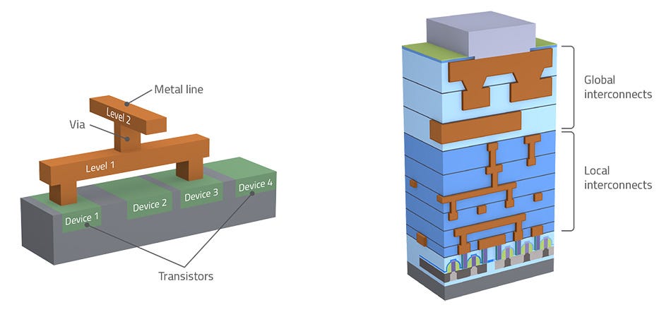
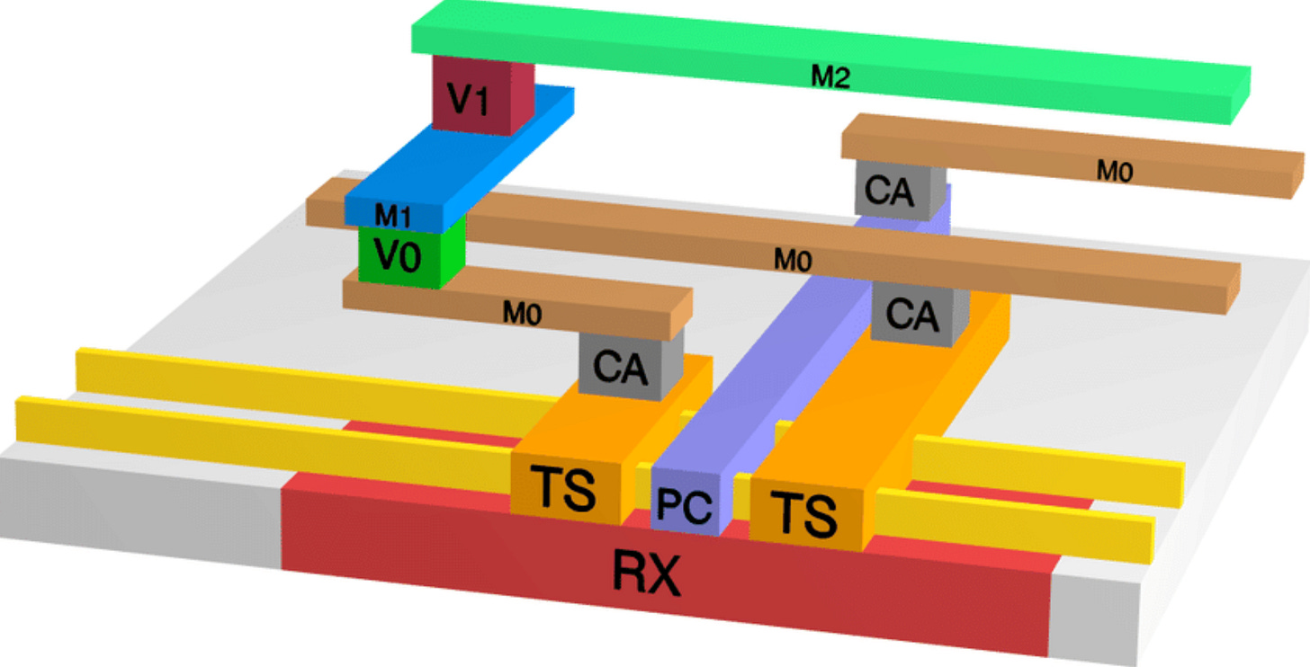
The metal stack is one of the most important parts of any process node. It is what enables routing signals around a wafer. The metal stack has more than a dozen layers that compose it, but the most important layers are the layers M0 to M4. In terms of layout on modern process nodes, the M0, M2, and M4 are critical metal layers that are perpendicular to the gates and M1, and M3 are parallel to the gate.
The metal stack of a chip is an area with many complex and difficult tradeoffs. The denser and thinner you make each metal layer, the more routing of signal can be done, and ultimately, the more useful transistors can be fit into any given area. However, this comes at big cost.
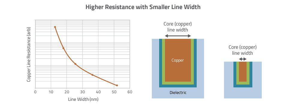
The thinner you make a metal wire the higher resistance that wire will have. Remember Ohm’s law from high school. Ohm’s law states that R = (V/I) where R is resistance, V is voltage, and I is current. Although Ohm’s law does not hold exactly true with such small wires, process node integration engineers must grapple with increasing resistance of a circuit for denser metal layers. They can compensate by increasing the voltage or reducing the current. The simplified tradeoff is that a denser metal stack costs more power to send a signal versus a more relaxed metal stack. It is not always a good thing to shrink the metal pitches.
Copper is the metal of choice for 3nm and 4nm process nodes from Intel, TSMC, and Samsung. With single patterning EUV, ~32nm is about the limit for line spacing with current resist chemistries and overlay capabilities. For vias this number is actually higher. For simplicities sake, let’s say the limit for EUV single patterning is 30nm for all features.
This example is incredibly oversimplified for demonstrative purposes. The image above is a single metal layer on a chip. Each 30nm by 30nm cell that the single patterning EUV tool can define, can be either copper, or an insulator, usually SiO2. This isn’t how lithography works, but it makes it easier to explain.
If one uses EUV single patterning, the metal layers could look like the above. There are many wires running around taking signal from one part of the chip to another. These wires also connect up to the layers below and above the layer of the chip we are looking at. In many cases, the layer has vias which are passing signal directly up and down to other layers without routing a signal. In this example, there is a big tradeoff in resistance as the metal is only 30nm wide.
This is where multi-patterning comes in. The goal is not to pack more wires in, but instead to maximize the copper area and minimize the SiO2 area. This would enable lower resistance and therefore higher performance and power efficiency when sending signals throughout the chip.
For simplicities sake, let’s say the limit of multi-patterning is now 15nm instead of 30nm. In reality, the current limit of LELE EUV is more in the range of ~21 to ~23nm. The upper bound is TSMC’s pitch on the M0 metal layer for their N3E process node. The lower bound is the 2nm class node we will discuss later. Just to note, multi-patterning doesn’t halve the pitch directly due to some margin being given up due to stacking overlay errors and stochastics.
If our pixel size is now 15nm, with multi-patterning in this oversimplified demonstrative imaginary example, the routing density would remain the same. Instead, this increase in fidelity would be used to deposit proportionally more copper relative to SiO2. The copper line width improves from 30nm to 45nm and the tip-to-tip spacing improves as well. The SiO2 insulator is still there to prevent the copper signals from intermixing and shorting the chip.
The increased line width and tip-to-tip spacing leads to a massive decrease in resistance and improvements in power and performance. Note that tip-to-tip and line pitch do not both improve with the move from single patterning to SALELE or pattern shaping, this example is exaggerated and unrealistic to show the potential benefits conceptually.
In the real world, the benefits are smaller, but needed, and one of the primary use cases of pattern shaping. The density of features is such that can already be achieved with single patterning, but the shapes of those features cannot. Pattern shaping helps bring the features that lithography can print, to the shapes the fab desires.
There is also a yield and power tradeoff with regard to metal layers and via layers. Vias are how the different metal layers are connected. Each layer is fabricated then stacked perfectly on top of each other. Process margin and overlay determine the ability to stack these up perfectly.
Any misalignment could cause a layer to miss the one below it so that no connection is made where there should be one (opens). Even worse, the metal layer could connect with another layer it isn’t supposed to, creating incorrect connections (shorts). Because pattern shaping is a selective process, the fab can tune up or down the directional etch in the direction or amount they need to minimize shorts and opens while maximizing size of the feature.
Resistance issues are very significant, especially on the lower vias where pattern shaping would be the most applicable. On TSMC’s N3E node, over 90% of via resistance is caused by V0 through V5.
The next 9 vias are quite insignificant as far as via resistance goes. If the V0 through V5 vias could be made larger, but still fit inside the same area, then resistance would decrease, and density would not be impacted.
The tradeoff of better fidelity from multi-patterning is great from a power and performance perspective for the metal stack, but it hurts significantly from a cost perspective. The number of process steps per metal layer nearly doubles.
Pattern shaping cannot increase the number of metal layers or vias in a given area, but it can increase their size and reduce the tip-to-tip spacing. The first use case is being implemented on a node going into volume production in late 2024 / 2025 for the metal stack.
The 2nd half of this report will be for subscribers. We will discuss and quantify the impact on EUV multi-patterning and High-NA EUV. We will discuss how Sculpta’s use cases could be evolved with future process technology scaling. A cost comparison for a real process node using EUV or a mix of EUV and Scuplta will be shared. We will also disclose the tool’s throughput, cycle time, cost, our shipment estimates, and our revenue estimates from customers.
We will directly discuss TSMC, Samsung, and Intel’s adoption and insertion points for Centura Sculpta. This will include specific process node details including minimum pitch and layers for an upcoming process technology that will use Applied Material’s Sculpta. There are pro’s and con’s.
We will also share the impact on other process steps including lithography, photoresist, coater/developers, CVD, PVD, etch, CMP, epitaxial growth, ion implantation, metrology, and inspection from the introduction of a new pattern shaping step. Pattern shaping has many ramifications for suppliers in the industry including but not limited to ASML, Lam Research, Tokyo Electron, JSR, TOK, Shin-Etsu, Lasertec, KLA, Onto, Nova, Hoya, and Asahi Glass.


