Going Vertical: Gate All Around, 3D DRAM, 3D NAND - Kokusai Electric IPO
Kokusai Electric IPO, 2024 to 2026 WFE Share, Memory Pricing, Atomic Layer Deposition (ALD), ASM International, Tokyo Electron, Applied Materials, Lam Research, Deposition Process
There are very few remaining large private semiconductor equipment companies, and the two largest that stand out are Kokusai Electric in Japan and EV Group in Austria. Both are amazing firms that are levered to trends in Gate All Around logic and 3D NAND. In the case of EV Group, the picture is quite simple, wafer bonders for heterogenous integration and backside power delivery.
Kokusai Electric (‘KE’) is IPO’ing soon, so it warrants a much deeper dive. Today we will dive into the manufacturing process for FinFET, DRAM, and 3D NAND as well as coming changes to that process flow with Gate All Around, CFET, and 3D DRAM. These scaling trends specifically affect deposition, lithography and etch heavily. This dive will also be meaningful for Lam Research, ASMI, Tokyo Electron, and Applied Materials. ASMI specifically pushes a narrative, that KE shows, isn’t exactly true.
In addition to the specific technology trends, we will also be sharing our view on DRAM pricing, NAND pricing, wafer fabrication equipment spend for 2024, 2025, 2025 by NAND, DRAM, Foundry/Logic, and Other. We have used our industry semiconductor equipment, model to flow through the future financials and will share Kokusai Electric valuation and forward estimates. This is a very significant IPO to pay attention to. For those that don’t need the deep dive on the tech, executive summary with comps and fins at the end.
Let’s start by going over the recent history of the firm.
A Trip Down Memory Lane
Kokusai Electric (‘KE’) was, for a long time, a part of the Hitachi conglomerate, formerly known as Hitachi Kokusai Electric (HKE). In March 2018, it listed separately on the Tokyo Stock Exchange (TYO:6756). HKE had two main business groups, semiconductor Thin-Film Deposition Process Solution and Video and Communication solutions. These two groups had completely different business models, products and client sets.
In 2016, HKE decided to restructure the company by spinning out each segment to different private equity investors. A few players joined the party, private equity firm KKR, HVJ Holdings, and JIP. In 2017, Private Equity firm KKR acquired Hitachi Kokusai, paying $2.3B for the entire business. The Thin-Film Process Solutions remained 100% owned by KKR, while the Video and Communications business was split into a separate company.
Shortly after, in July 2019, Applied Materials (AMAT) announced they wanted to acquire the new Kokusai Electric (i.e. only the Thin-Film Process Solutions Business) for $2.2B (and then subsequently raising the offer by 59% to $3.5B in 2021). The acquisition was subject to antitrust clearance and after two years of awaiting approval from China’s authorities holding up the process, AMAT aborted the acquisition.
After five years of ownership, KKR has turned to an exit via KE’s IPO, in which KKR will sell 30% of KE’s shares in an all secondary deal, with no additional shares being issued or capital being raised by KE.
Thin-Film Deposition – Batch ALD Specialist
Kokusai Electric (‘KE’) is positioned as a specialist in the deposition of thin films. Specifically, KE sells batch deposition tools with a specific focus on batch Atomic Layer Deposition (ALD), the most selective/precise form of deposition. KE also has a presence in surface treatment, though in terms of revenue exposure for this is a distant second to deposition.
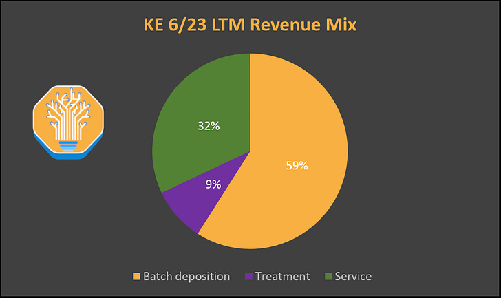
Around 30% of their revenue is also service related, but it should be noted that within KE’s service segment, there is a portion of legacy 200mm equipment sales. This means that KE currently has lower service intensity compared to the other deposition players, which is good for fabs total cost of ownership (TCO), but maybe a drag on financials. With that said, KE’s new mini-batch tool is 4x the service attach rate and the best TCO tool they’ve ever released.
KE is more memory focused. NAND is their largest application for their equipment, followed by DRAM and then logic. This likely begins to shift with the adoption of Gate All Around. We will go through more on that later.

KE’s specialty is not involved in all Chemical Vapor Deposition (CVD) and Atomic Layer Deposition (ALD) but specifically batch CVD/ALD tools. The other major toolmakers (Tokyo Electron, Applied Materials, Lam Research, ASMI) all offer ALD tools but they mostly focus on single wafer offerings, IE processing 1 wafer per chamber instead of multiple (batch). KE dominates the batch ALD process with ~70% market share, the remainder belongs mostly to TEL (and ASMI having a slither).
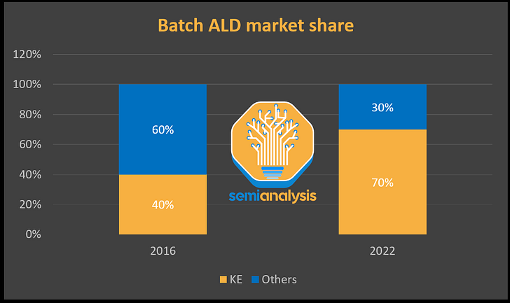
While KE emphasizes their share in ALD, they still have exposure to batch CVD tools. KE’s blended market share in batch deposition is “only” ~46% (compared to ~70% in batch ALD). TEL is only slightly larger in the total batch deposition market, but we believe that will flip soon and KE will become larger.
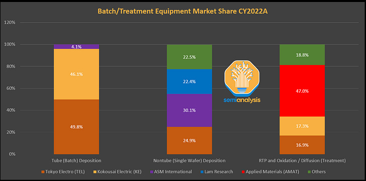
This is a very strong position in the market, and explains why Applied Materials wanted to acquire KE. AMAT already has a strong ALD portfolio. AMAT has a number of Processes of Record (POR) for next generation Gate All Around (GAA) logic ALD steps despite the market’s impression that ALD leader, ASMI, is going to completely dominate and continue to grow share.
AMAT’s expertise lies in single wafer processing, and they wanted to add KE’s batch capabilities to their portfolio. To be clear, batch ALD vs single wafer ALD are separate capability altogether. Expertise in single wafer ALD doesn’t necessarily transfer directly to batch ALD tool production. AMAT’s attempted acquisitions are effectively an endorsement of KE’s proficiency in this subsegment. Next, we dive deeper into the underlying technology behind KE’s products: deposition, ALD, and batch processing.
Deposition - The Basics
Deposition, as the name suggests, is the process of depositing of a particular material onto the wafer. While we refer to chips as “silicon” because the base substrate used for chip fabrication is silicon, there are in fact many different materials present on a fabricated wafer. It is via deposition that these materials (usually different metals and oxides) are placed onto the wafer.
There are a few forms of deposition that are used to deposit different materials: Electrochemical deposition (ECD) also known as electroplating, Physical vapor deposition (PVD), and chemical vapor deposition (CVD) of which Atomic Layer Deposition (ALD) is a subset. Let’s go over a quick overview.
Electrochemical Deposition / Electroplating
Electroplating is a common technique used to deposit metal films onto another metal surface, and the basic concept remains the same in semiconductor manufacturing. Electroplating is commonly used to deposit copper, for example to build interconnects for the metal layers, or to fill though-silicon vias. The wafer and copper source are placed in a bath of a liquid that is electrically conductive. Both the wafer and source are connected to a power source. Current is applied and the flow of current from the power source dissolves ions from the source and deposits the source ions onto the wafer.

Physical Vapor Deposition / Sputtering
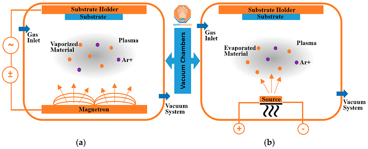
Physical Vapor Deposition (PVD) creates a metal vapor from a target material by using plasma (in a similar mechanism to a plasma etch). The kinetic energy of the plasma sputters the target material to land on the wafer and be deposited. PVD is often used to deposit barriers and copper seeds for metal interconnect layers, and various forms of nitride liners.
Chemical Vapor Deposition
The most common type of deposition used is Chemical Vapor Deposition (CVD). CVD is often used for dielectrics and other metals. In CVD, multiple precursor gases are emitted into the chamber. These gases are diffused onto the wafer where a chemical reaction occurs to form the material that is deposited onto the wafer.
For example, silicon (di)oxide is a common dielectric/insulating material. To deposit silicon oxide, one method is to combine the precursor gases of Silane and Oxygen which reacts to produce of silicon dioxide and a hydrogen by-product
SiH4 + O2 → SiO2 + 2 H2
Atomic Layer Deposition
Atomic Layer Deposition (ALD) is a subset of CVD. In ALD, each precursor gas is emitted one at a time. The first gas is emitted to coat the wafer. An inert gas (such as N2 or Argon) is then flowed into the chamber to purge any excess of the previous precursor gas and any by-products. Then the second reactant gas is flowed in. An atomic layer of the second reactant attaches to the surface of the wafer where a layer of the first reactant and these elements will react to create the target material. This process is repeated to create a film of the desired thickness.
The key feature of ALD is that it is a self-limiting process. Only one single layer of atoms is deposited at a time. Once the surface is saturated, the precursor cannot be deposited anymore. This is what makes ALD attractive as a deposition method.
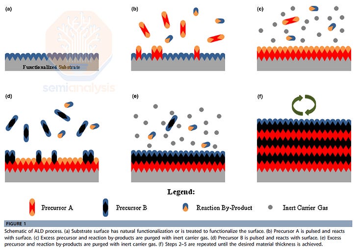
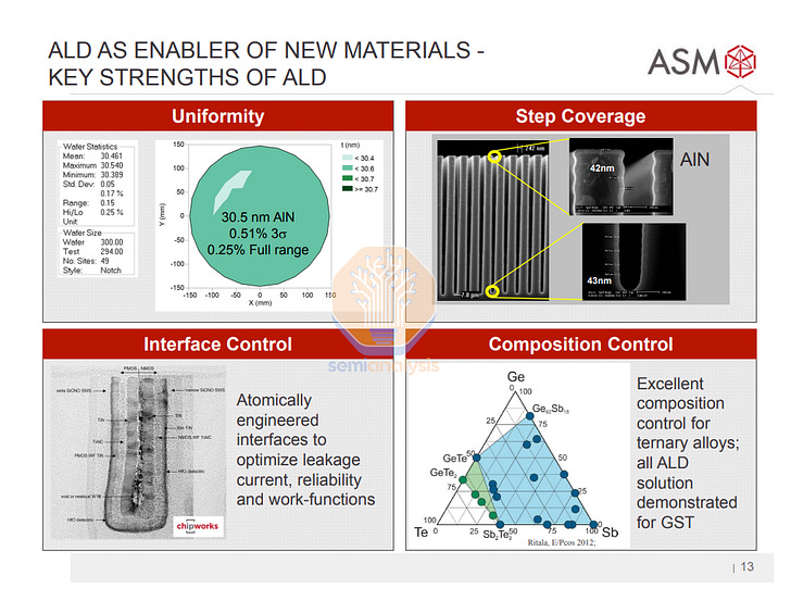
It results in films that have very high conformality, step coverage, no pinholes, and allows for precise film thickness control. These are all common defects that other forms of deposition face. ALD is especially important for more challenging deposition tasks: very thin film depositions and deposition on surfaces with complicated topography (ie. non-planar surfaces) such as 3D or very high aspect ratio structures.

Basically, ALD is superior in terms of deposition quality compared to conventional CVD in every single way. The catch 22 is that ALD throughput is much lower, IE costs more floor space, tool time, and money. Only one gas precursor is being emitted at a time, and then the purge processes to get rid of excess precursor and by-product also adds additional process time. This involves multiple steps as compared to traditional CVD which is accomplished in one step. All this only results in a single atomic layer being deposited. This is less of a problem for very thin films but makes ALD less attractive for thicker films. To address poor throughput, one solution is to batch this process.
To batch or not to batch? That is the question.
Instead of processing one wafer at a time, batch tools can process multiple wafers (sometimes 100s of wafers) to increase throughput. As mentioned, it is KE’s batching capabilities that sets them apart from the crowded field of ALD suppliers (ASMI, Lam Research, Applied Materials, Tokyo Electron).
The benefits of batching are obvious: process more wafers at a time, resulting in higher throughput and lower tool cost of ownership. However, there are several downsides to batching. With batching, it is hard to control process conditions because the chamber is much larger. In addition, with multiple wafers in the chamber, there can be more undesirable interactions leading to defects. If anything, batching was more prevalent historically in the early days of the semiconductor fabrication. The steady trend over time has been more use of single wafer tools as they offer more control and flexibility in a world where leading edge processes have ever tighter process tolerances.
For a process like ALD, batching offers a huge advantage as it helps address the key drawback of ALD: low throughput. Meanwhile, ALD also has self-limiting characteristics as we discussed earlier, making control inherent to the process and offsetting the higher defectivity that batch processes can bring.
Another point to note on batching is that it is suited to processing a high number of homogeneous wafers, which is the case in memory but not logic. In logic, while the largest volume chips do demand thousands of wafers a month, and in some extreme cases, tens of thousands of wafers, but it’s also very common to run dozens of wafers at a time of any particular design. This means that batch tools couldn’t even be saturated, and mixing designs mean the process cannot be optimized to that particular wafer’s data gathered from metrology/inspection.
Putting aside accuracy, the first question to answer is if batching is actually more productive than single wafer? If not, then batching is pointless. While it would seem intuitive that batching 100 wafers at a time is more productive than processing one wafer at a time, the reality is not so simple. Batching comes with a lot of additional overhead that adds to cycle time compared to single wafer processing. For example, batching uses a much larger process chamber, so it takes much longer to get that process chamber to correct process parameters such as temperature and much longer to normalize to the fab environment after deposition.
This additional overhead is more effectively amortized when the equivalent single wafer deposition process has a longer process time, which is what would make batching more effective than single wafer. Put another way, wafers that have characteristics required for certain features that add to deposition cycle time, which makes it more likely to see productivity benefits by batching.
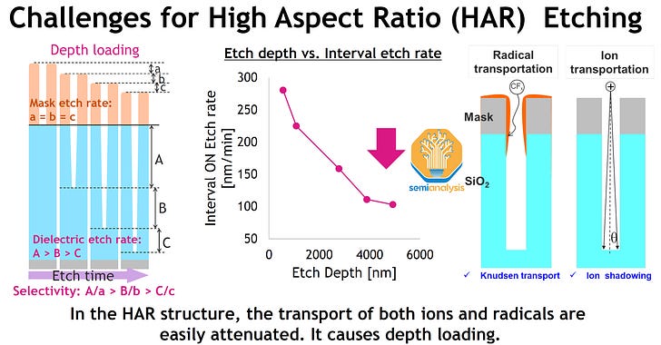
Primarily, the main feature that adds to deposition time is high aspect ratio (‘HAR’) structures. Aspect ratio is the ratio of height relative to width: so deeper and narrower structures are considered to be high aspect ratio structures. HAR structures drastically increase the exposed surface area that needs to be deposited. In the same way a larger wall will take a longer time to apply a fresh coat of paint, a larger surface area will take longer to saturate with atoms.
Another reason is depth loading, which we discussed as a challenge for NAND etching and why Tokyo Electron can gain share from Lam Research in 3D NAND. The same principle applies to deposition. Basically, it takes much longer for a gas to penetrate a deep and narrow trench. However, unlike etch, the solution isn’t performing the process in cryogenic temperatures as ALD needs to happen at above room temperature.
KE has a large batch tool, the AdvancedAce which can batch up to 175 wafers at a time (this is just for CVD not ALD) and the Tsurugi which is actually a “mini-batch” tool that can batch up to 50 wafers at a time. The reason for mini-batching is that it is a smaller chamber that takes less time to reach the process parameters such as heating up and cooling down and offering a higher gas flow rate than the larger chamber. This may provide a better balance of overhead time and deposition time to optimizes for final throughput.
We commonly see high aspect ratio structures in memory as opposed to logic. In the case of NAND this is the channel hole with an aspect ratio of >70:1. DRAM also has high aspect ratio trenches for capacitors.

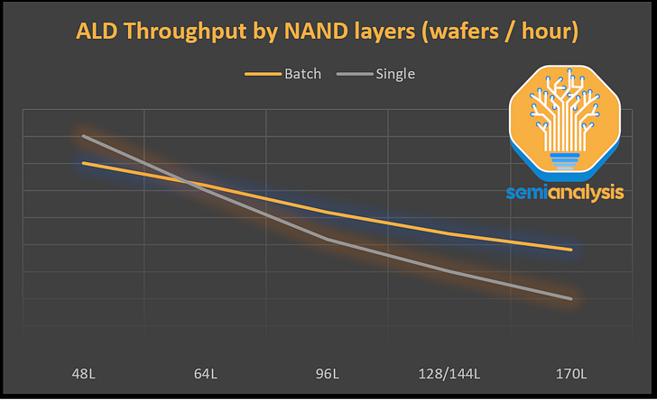
Case in point is that batch ALD has lower throughput than single wafer for 48-layer 3D NAND, due to process throughput being high enough. Due to depth loading, the two become on par at 64-layer. Beyond that, batch has become more productive for higher layers with the gap between the two widening. Why? More layers mean higher aspect ratio channel holes. Higher aspect ratio holes mean a longer process time. Longer process times flip the throughput equation in favor of batching over single-wafer.
There are also other factors that make batch more prevalent in memory. Batch tools see higher downtime as the chamber only runs once full. Wafers can sit idle in the process chamber as they wait for other wafers to go through other preparation steps before deposition. This is less of a problem in memory as there will be high homogeneity of wafers vs a logic foundry that is running multiple different wafers.
For logic, the flexibility and fast cycle time of single use tools allow more variation of process conditions for faster R&D and prototyping. In many cases, a foundry will want to run just a few wafers through, a concept called hot lot which is something Intel used too much costing them billions. This reduces utilization, but gets design teams and yield teams their data as soon as possible. Iteration on a design, qualifying samples, or tweaking process parameters to increase yield is a constant battle on logic.
Memory fabs are far more cost sensitive compared to logic and foundry as memory is a commodity product. At the end of the day, cost is the only differentiator for commodity products. In memory, the process is fine-tuned, then you run hundreds of thousands of that product for years.
Also, memory wafers are much cheaper compared to logic wafers. Leading edge logic wafers are in the region of $20,000 each, if 175 of these wafers are batched and the process doesn’t work properly, that’s very expensive.
ALD Applications
Where is ALD best used? In general, ALD is used on structures that have a complicated topography, especially anything that is high aspect ratio or 3D, or for very thin films. For critical films, the key is achieving good “step coverage”: that is ensuring the deposition has uniform thickness across an uneven substrate. When processes get more 3D, step coverage is harder to achieve. If you are trying to fill in the walls of a deep trench, it’s very important the bottom gets filled at the same rate as the walls near the mouth of the trench.
Today, all NAND flash is 3D, so we see a lot of ALD used for it. Logic is becoming more 3D with gate all around structures and 3D DRAM on roadmaps. Structurally, this means higher etch and deposition intensity overall. Likewise, lithography intensity has fallen for 3D NAND.
ALD in particular sees more use. There are more and more different films being used, and these films need to fit in small feature sizes and on more complicated topographies. We will go through some examples of ALD applications in 3D NAND as well as upcoming uses in Gate All Around logic.
3D NAND Usage of ALD
Let’s revisit the 3D NAND process flow which we previously wrote about:
Alternating layers of Oxide and Nitride films are first deposited onto the base wafer. Each layer is between 20 to 30 nm in thickness. The theoretical limit per stack can be over 250 layers high and nearly 7 microns tall. A thick hard mask is then added to prepare for the High Aspect Ratio (HAR) channel hole etch. This Reactive Ion Etch process digs an array of holes 70 times deeper than wide. Channel hole uniformity in roundness and across the entire depth of the hole is crucial in reducing memory cell performance variability. These steps are repeated for designs with multiple decks that are then stacked on top of each other.
From this, the channel holes are filled with multiple layers to form the charge trap cell, with each layer deposited on the sidewalls making the hole progressively narrower. Next comes the metal replacement gate process. Slits are etched down though all layers to form trenches that expose the sides of the stack. This allows access for the exhumation of the Nitride layers and subsequent deposition of barriers done through ALD and the Tungsten Word Line fill. Staircases are etched on the sides of the array to expose the Word Line layers to vertical contacts.
Finally, the Bit line and metal interconnect is formed above and connects with the fabricated CMOS circuits, which include Word Line drivers and other peripheral circuitry for the NAND interface. From this, we see that 3D NAND is highly dependent of HAR etch and deposition capabilities to scale density and performance.
Etch gets a lot of attention for NAND, but notice there’s a lot of deposition too.
This image below is cross-section of a 3D NAND memory cell. You can see that there are a lot of different materials used. There are six thin films that require ALD: blocking oxide, charge trap nitride, tunnel oxide, channel silicon. This is in addition to the base silicon layers and the Tungsten fill in the wordline. For the blocking oxide, charge trap nitride and tunnel oxide, KE’s batch ALD is the process tool of record among ALL of the top 5 NAND players. For channel silicon, blocking metal and barrier metal, KE has some presence here and there, but really KE dominates the first 3 steps.
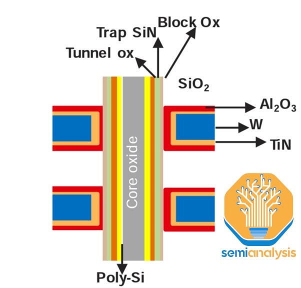
Often, when the topic of competition between semicap makers comes up, we say that the market is complicated. It is difficult to categorize deposition as just one market as there are many different subsegments and niches, each with their own leaders.
There is a lot less competition that people realize. This is a great example. For these few specific NAND deposition steps, KE clearly dominates.

DRAM Usage Of ALD
In DRAM, the high aspect ratio feature is the capacitor. Each bit of data is stored in the capacitor as either a negative or positive charge. Each capacitor is connected to a transistor which controls access to the data in the capacitor. This is the one-transistor, one-capacitor (1T1C) memory cell architecture that DRAM is based on.
The capacitor itself is a long cylindrical structure that has a high aspect ratio. It is filled with a metal-insulator-metal stack. The insulator is a high-k zirconium dioxide to prevent leakage while maintaining capacitance. It is this MIM stack that requires ALD due to the need for a well-controlled, conformal film in a high aspect ratio structure. This is the step where KE has a strong presence in DRAM. For example, we know that KE’s batch ALD is used for certain parts of the high-k deposition with Samsung and potentially with other DRAM makers as well.
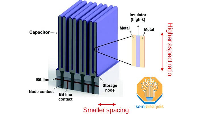
Currently, the key challenge to scaling DRAM further is scaling the capacitors. Any further shrink of the capacitors will render the capacitors unable to hold a charge and therefore useless. Like NAND, 3D DRAM is being proposed as the future architecture to enable continued cost scaling.
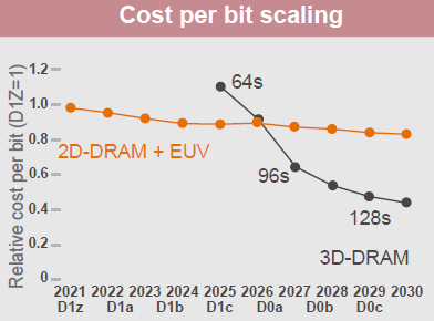
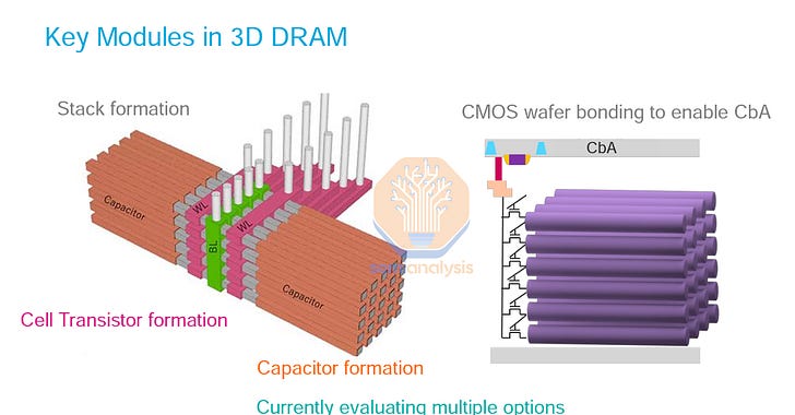
Most equipment makers think 3D DRAM will be in mass production in the second half of the decade (except ASML who insist on it being well beyond 2030). It is not yet settled what the exact 3D DRAM architecture looks like as there are few potential workable architectures. It is an opportunity for ALD and etch, but it is also be a threat for certain tool makers as it will result in a reshuffling of market share.
Logic Usage Of ALD
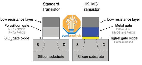
ALD’s first major entry into logic fabrication was in 2007, when Intel introduced ALD in their 45nm process in 2007. Previously, silicon dioxide was used for the gate insulator. As feature sizes shrank, so too did the silicon dioxide layer, but it was found that at around 2nm thickness, silicon dioxide was failing to insulate current properly.
It was Intel’s 45nm node that introduced the revolutionary High-K Metal Gate (HKMG) structure that substantially reduced current leakage and a key enabling feature for scaling beyond the 65nm node. The HKMG structure replaced the traditional insulating silicon oxide with hafnium oxide and used a metal for the gate instead of polysilicon. The High K dielectric was enabled by use of ALD. The hafnium film needed to be highly conformal, pinhole free, with tight thickness control to achieve its insulating purpose which was a task very well suited for ALD. In addition, ALD also won out because the more standard CVD process left excess particles for hafnium oxide deposition.
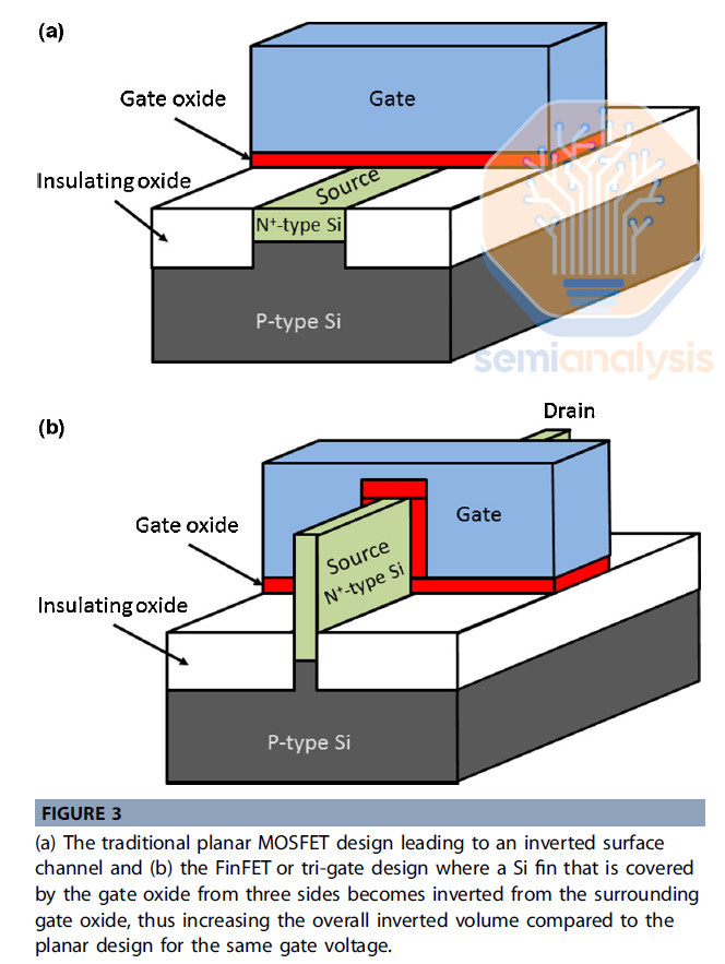
Then, as logic entered the FinFET era with transistors becoming 3D as opposed to planar, the need for ALD increased further. We can see for a FinFET, the gate wraps around the channel on three sides which protrude as fins. The effect is that the gate can better control current flow through the transistor so that leakage is reduced, and a lower voltage is needed to power the transistor. The gate oxide also wraps around and is no longer a planar film anymore, this makes achieving step coverage more difficult. While already a task that was handled by ALD, we can see that this new more challenging topology only makes ALD even more well suited for the task.
Overall, in logic we don’t see structures anywhere near as high aspect ratio as in memory. Still, batch ALD is used with TSMC being KE’s second largest customer. There are films that need ALD but are simpler (as opposed to the very complicated and critical films where an ASM single wafer tool be used) and are reoccurring processes that would be required multiple times per wafer making batching beneficial when considering the total cost of ownership.

In this case, KE and TEL’s batch ALD tools are more of the workhorse deposition tool compared to a specialized single wafer tools from ASMI, Lam Research, and AMAT. One such example is batch ALD is used for deposition of the spacer that is on the sidewalls of the FinFET gate. The purpose of the spacer is to reduce the capacitance between gates and is a low-k film. As you can see, the spacer needs to be deposited on top of the protruding gate which is relatively higher aspect ratio compared to the high-k dielectric between the gate and channel.
This is where batching and KE’s tools are present in logic. Another feature Batch ALD is well suited to is gap fill for trench isolation. Shallow trench isolation is a technique used to prevent unwanted electromechanical interference and parasitic leakage between individual circuits. Trenches are created via an etch process and then filled with a dielectric like silicon dioxide which can be completed via batch ALD.
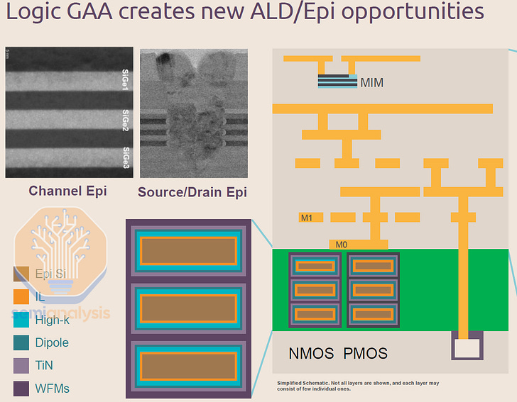
With FinFET, we saw that wrapping the gate around the channel on 3 sides improved electrical characteristics, so wouldn’t coverage on all four sides be even better? Basically, yes it would be better. This is the approach for next generation Gate All Around (GAA) transistor architecture. The channel becomes a series of multiple vertically stacked nanosheets inside the gate. The gate now wraps around the channel in all four directions as opposed to just three in FinFETs, allowing for even greater drive current and leakage control for improved power consumption.
Looking more closely at the gate, it is actually a high-k metal gate stack that surrounds each nanosheet (denoted in the below diagram as the “Epi Si”). There are several dipole and work function metal layers that are needed to control threshold voltage.

ALD is a must to deposit these very films as they must be thin to all fit inside such an ever shrinking gate. With this, it becomes quite clear that GAA will require several more ALD steps compared to FinFETs.
In the rest of this report, we will talk about where single wafer vs batch ALD is being used in the Gate All Around. We will also go over the CFET process. We will also discuss whether KE, ASM International, TEL, AMAT, or Lam Research have won share in those steps. We will also go over KE’s treatment business and trends/leverage there.
In addition to the specific technology trends, we will also be sharing our view on DRAM pricing, NAND pricing, wafer fabrication equipment spend for 2024 and 2025 by NAND, DRAM, Foundry/Logic, and Other. We have used our industry semiconductor equipment model to flow through the future financials and will share Kokusai Electric valuation and forward estimates. This is a very significant IPO to pay attention to.


