TSMC 3nm FinFlex + Self-Aligned Contacts, Intel EMIB 3 + Foveros Direct, AMD Yield Issues, IBM Vertical Transport FET (VTFET) + RU Interconnects, CFET, Sequential Stacking, Samsung Yield, and more
IEDM 2022 Round-Up
We recently attended the 68th Annual IEEE International Electron Devices Meeting in San Francisco. IEDM is a premiere conference for state-of-the-art semiconductors device technology. In 2022, countless companies, from the likes of Intel, TSMC, Samsung, IBM, Micron, Unimicron, ASE, and Applied Materials to research institutions like IMEC and CEA-Leti, and many universities presented on the leading-edge of semiconductors. The leading-edge does not just refer to the most advanced logic processes, but also memory, analog, packaging, and many other fields. It is important to stay on top of this conference as it shows technologies that will lead to changes in business across equipment, foundry, fabless, device, and packaging.
This article is the first part of a short series about the many advancements, developments, and research talked about at IEDM, which will cover advanced logic technologies and advanced packaging. This article will cover CFET, the next evolution of gat all-around transistors, Sequential Stacking, LFET, Applied Materials Barrierless Tungsten Metal Stack, Samsung Hybrid Bonding Logic 4um and HBM, ASE FoCoS, TSMC 3nm FinFlex and Self-Aligned Contacts, Intel EMIB 3 and Foveros Direct, Qualcomm Samsung 5nm DTCO & Yield, IBM Vertical Transport FET (VTFET) and RU Interconnects.
We will also discuss some AMD Yield Issues that cropped up, unrelated to any of the presentations/papers at IEDM.
If you enjoy it, please do share, subscribe, and let us know, this took a tremendous amount of work, and we know this is too technical for most subscribers. Even if you believe it is too technical, at least scroll through, there should be some interesting bits.
TSMC FinFlex - Paper 27.5
At IEDM 2022, TSMC talked about N3B and N3E, as we detailed previously. We discussed a lot around cost, performance, the Contacted Gate Pitch (CGP), Minimum Metal Pitch (MMP), and SRAM bitcell size, but these were far from their only contributions to the conference.
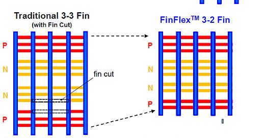
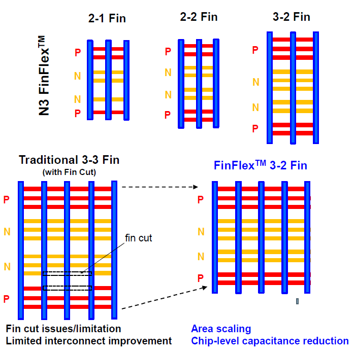
In TSMC’s paper on N3E, they introduced FinFlex. This is part of the immense design technology co-optimization (DTCO) that went into the N3 family of nodes. FinFlex is an advanced form of fin depopulation. Usually, with fin depopulation, the number of NMOS and PMOS fins is reduced in a standard cell. This allows the reduction of cell heights and, therefore, improvement in density. With more advanced nodes, each fin can also carry more drive current, allowing fin depopulation to occur with little impact on performance.
However, with reduced cell height, the interconnect becomes a more limiting factor. With a 1-fin cell, there is little room for interconnects, and the interconnects becoming the sole bottleneck is almost guaranteed. With FinFlex, a 2-1 fin setup is used, where a 1-fin cell is stacked on top of a 2-fin cell. This helps alleviates the interconnect bottlenecks and effectively results in a cell with a height of 1.5 fins. With N3E, TSMC offers three libraries, a 2-1 cell library for high density, a 2-2 cell library for balanced power and performance, and a 3-2 cell library for high performance.
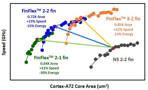
According to TSMC, the 2-1 cell library offers 30% lower power at the same performance, 11% higher performance at the same power, and a 36% reduction in the area relative to the 2-fin library on their N5 node. The 2-2 cell library offers 22% lower power at the iso-performance, 23% higher performance iso-power, and 28% lower area. The 3-2 cell library offers 12% lower power iso-performance, 32% higher performance iso-power, and 15% lower area.
N3E also offers 6 threshold voltage options, eLVT, uLVT, uLVT-LL, LVT, LVT-LL, and SVT. Each of these comes with different tradeoffs in power and performance and allows designers to tune their power-performance characteristics more precisely.
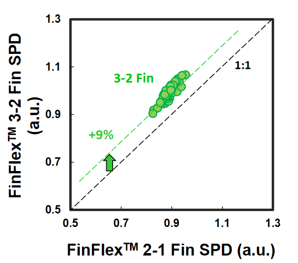
When comparing the 2-1 and 3-2 cells, TSMC shows the 3-2 cell has 9% higher performance. Unless the designers absolutely need this performance, the gains are minimal in performance. This strengthens the case for denser, more power-efficient libraries. However, that ignores interconnect density limitations. FinFlex lets designers achieve the highest density possible with denser cells with less dense cells, such as the 2-2 and 3-2 cells to maximize their interconnect routing and performance.
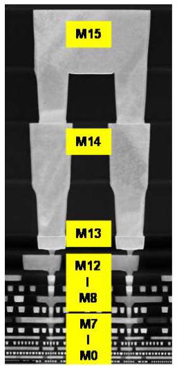
The metal stack of N3E, while slightly relaxed from N3B is still extremely dense. The metal 0 pitch is 23nm, an 18% reduction from N5. Double-width is also offered on the metal 0 layer for lower resistance and higher performance.
TSMC incorporated an innovative liner to the copper interconnects to reduce resistance on the lower metal layers. We believe this liner is Ruthenium, which Intel has also used as a liner in their 10nm node. This decreased contact resistance decreased by 20-30%, and via resistance decreased by 60%. TSMC also mentioned that three critical layers which required double-patterning with EUV on N3B have been replaced by single-patterning with EUV on N3E. This reduces complexity, costs, and improves cycle times.
N3E, when it goes into high-volume manufacturing late this year, will be the most advanced node in production. TSMC will continue its dominance on the leading-edge of logic. Innovations like FinFlex show that TSMC is forging ahead. It is quite annoying the lack of details TSMC shares. Intel had no issues detailing its own advanced Intel 4 node at the VLSI Technology Symposium earlier in 2022.
TSMC 3nm Self-Aligned Contacts (N3B) - Paper 27.1
Ever since TSMC’s transitions to FinFETs on N16, the profile of the fin has been crucial to improving performance and reducing power. Although TSMC was able to reduce the gate length from 16-23nm on N7 to 12-14nm on N3B, TSMC also mentioned that gate length scaling had reached its limit. Even with fin profile optimization, TSMC was unable to reduce this further. This further emphasizes the importance of Design-Technology Co-Optimisation (DTCO) to enable further scaling into the future. Furthermore, it was mentioned that the FinFET transistor architecture has reached its limit, and a move to nanosheet transistor architecture is essential.
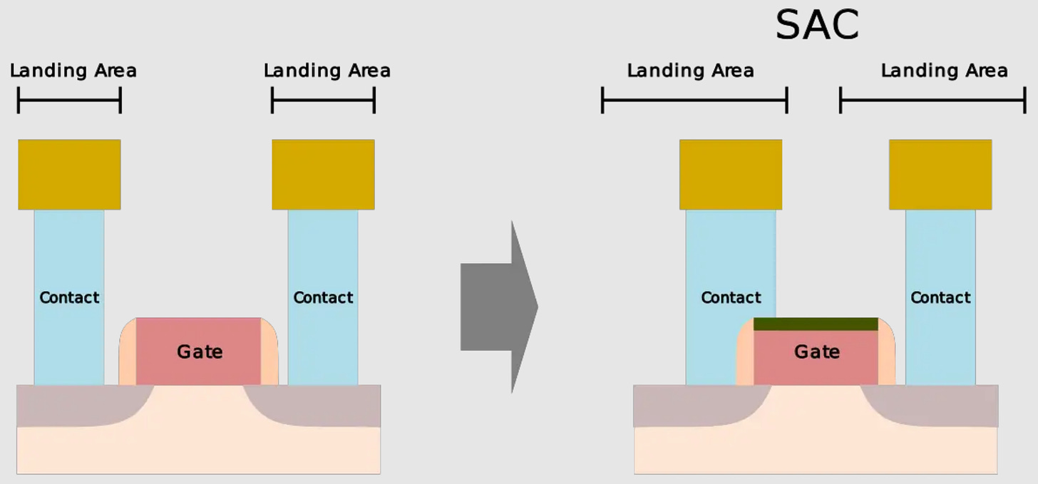
With N3B, TSMC also implemented Self-Aligned Contacts (SAC). This is very interesting because Intel has been implementing SAC since 22nm. Meanwhile, TSMC’s first node with this technology is N3B. Furthermore, they removed SAC in N3E.
Our friends over at WikiChip have a great explanation of the technology, but to summarize, due to scaling differences between the contact poly pitch and gate length, the landing area for contacts has shrank significantly. This is exacerbated by tighter alignment tolerances and overlay issues due to multiple masks.
SAC enables the contacts to even land on top of the gate without shorting the transistor. While this increases process complexity and therefore cost, it improves yields. Unfortunately, it also impacts performance as the gate-SD contact capacitance increases significantly.
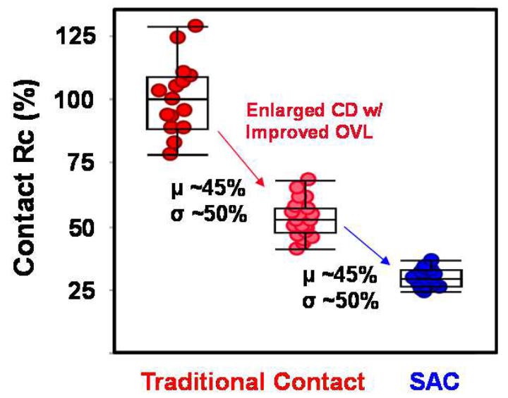
TSMC’s scheme on N3B allows for the leakage at the gate-contact junction to remain constant even at wider gate lengths and process variations where the contacts and gates are aligned to different parts of the gate. SAC also reduced contact resistance by 45% and variation by 50%. This allows for both better electrostatics and performance, and higher yields in manufacturing.
With the gap between the gate and the contact continuing to decrease and due to the FinFET structure, TSMC faced a problem of increasing capacitance at the gate-contact junction. Although a thicker spacer would have alleviated this, that brings other problems like higher contact resistance. Inevitably, TSMC looked to decrease the dielectric constant and utilize low-k materials. Although the k=1 of air was promising, TCAD simulations by TSMC showed that it would have a smaller impact than switching to a dielectric with k<4.0. This increased the maximum voltage by over 200mV and reduced the capacitance at the junction by 2.5%. These are just some of the minor details in optimizing a new process technology that can be overlooked.
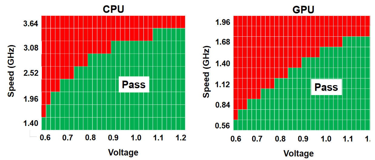
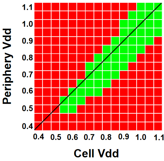
TSMC also showed shmoo plots of a test chip on their N3B node, which showed a CPU core reaching 3.5 GHz at 1.2V and a GPU core reaching 1.7 GHz at 1.2V. They also showed a shmoo plot of the SRAM in the chip, which was fully functional down to 0.5V.
Qualcomm & Samsung DTCO - Paper 27.4
At IEDM, Qualcomm and Samsung also talked about the DTCO used with the Snapdragon 888 on Samsung’s 5LPE node. Qualcomm states that the smallest fin pitch (FP), CGP, metal pitches, and SRAM bitcells were used to achieve a 25% shrink over 7LPP. These changes can be seen in the Ultra High-Density library of 5LPE. However, these shrinks also came with increased risks to the process.
From the start to initial production, Samsung reduced defects by 60% and further reduced this to 2% of the baseline by high-volume manufacturing. 5LPE also experienced excellent yield improvement, faster than 10LPE and 7LPP. Part of this is also due to 5LPE being an incremental improvement over 7LPP.
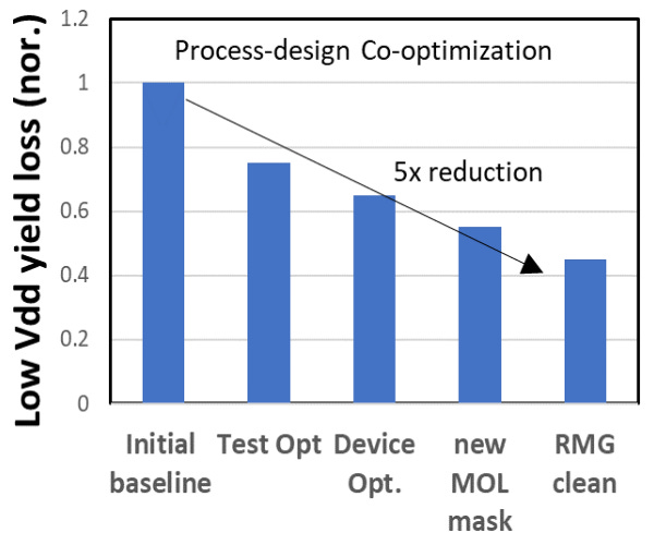
Qualcomm and Samsung also worked together with DTCO to improve yield greatly, achieving 2.5x lower yield loss for operations at low voltages, which is the primary use case of mobile SoCs. They also reduced the number of defective devices by 9x, which is very significant.
Through continued DTCO, Qualcomm and Samsung also reduced the CPU power draw by 7% and total power by 3%. As process node scaling slows, DTCO will become more and more important to achieving desirable characteristics for chips.
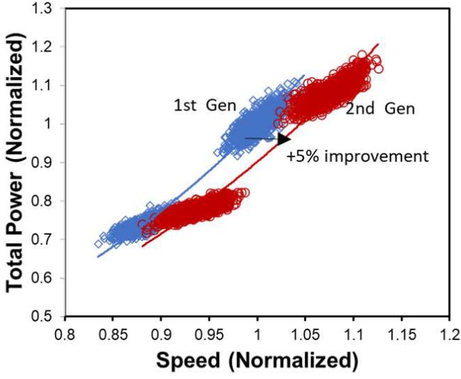
Samsung also compared their 1st generation node, 5LPE, to their 2nd generation node, 5LPP. They showed it achieved a 5% higher performance at the same power. 5LPP is also used in the Snapdragon 8 Gen 1, although marketed under the name of 4LPX.
Advanced Logic Technology —Transistor Architecture
After Gate All-Around FETs (GAAFETs) and maybe Forksheets, the industry will likely move to Complementary FETs (CFETs), where the NMOS nanosheets are stacked on top of PMOS nanosheets or vice versa. This is a difficult process because the P and N-type formation requires very high-temperature epitaxial growth. Whichever you make 2nd will result in high temperatures exposure for the 1st, which could destroy it. TSMC, Intel, and IMEC have all presented research on this. In order to fabricate CFETs, there are two methods, sequential and monolithic.
Heterogeneous 3D Sequential CFET with Ge Nanosheet p-FET by Direct Wafer Bonding - Paper 20.1
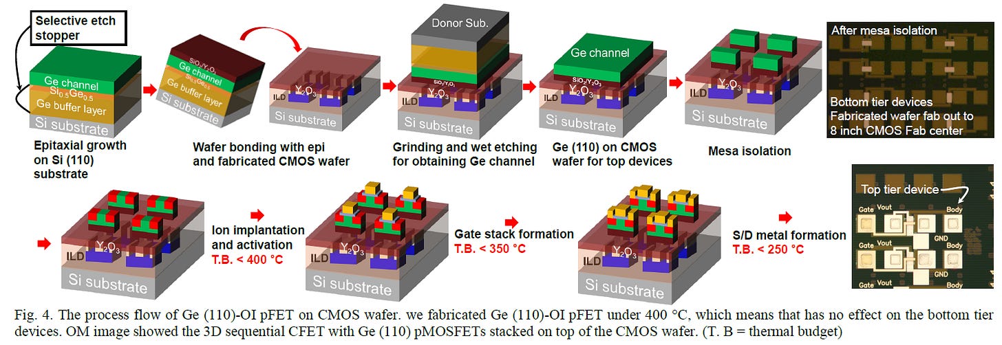
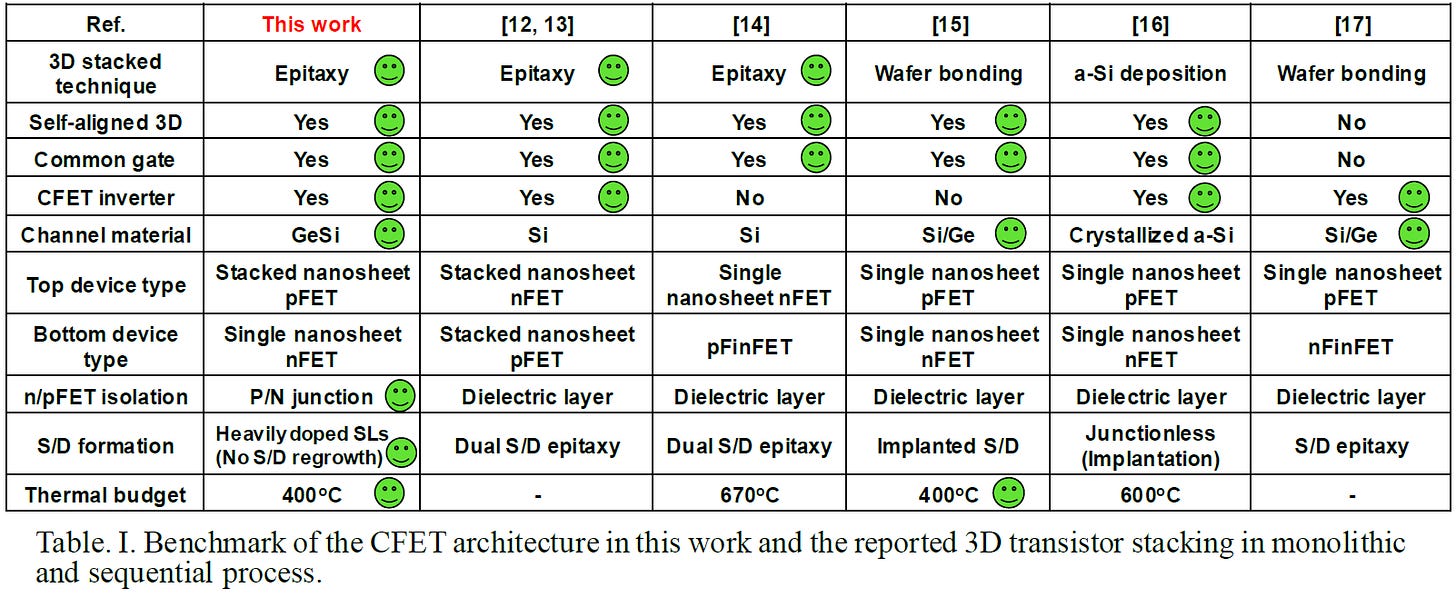
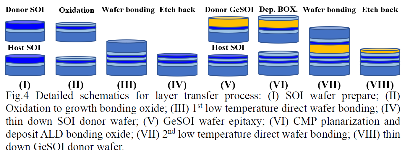
The Korea Advanced Institute of Science and Technology presented a method for sequential CFET fabrication. KAIST got around the temperature issue by going with a sequential stacking methodology where they perform the high-temperature epitaxial growth and then separately combine them together with wafer-to-wafer bonding. The bottom pFET consisted of Ge, while the top nFET consisted of Si.
This new method allows for a more preferable orientation of the Ge crystal lattice, which has a higher electron mobility. In recent leading-edge nodes, the drive current of the pFET has been especially problematic, and this is one approach to mitigate this problem. It was tested that the process of adding the top nFETs did not affect the electrical characteristics of the bottom pFETs.
Monolithic 3D Self-aligned GeSi Channel and Common Gate Complementary FETs by CVD Epitaxy - Paper 20.3
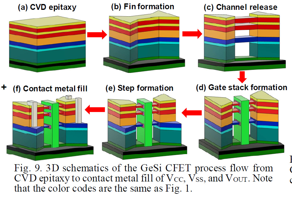
The National Taiwan University showcased their work on monolithic CFETs, IE without wafer bonding. This is possible with a low temperature (400C) epitaxial growth, which would prevent the prior structures which were made, from being destroyed. They fabricated SiGe channels with 75% Ge and 25% Si, and used a P/N junction to isolate the two halves of the CFET. With their method, they were able to successfully stack two pFET channels over 1 nFET channel.
While stacked pFETs on stacked nFETs have been shown before, this is the first time they’ve been shown with a P/N junction, and the process seems to have minimal impact on the formation of the source and drain. They claim this is an easier process to implement than previous approaches.
IBM Vertical-Transport Nanosheet - Paper 34.4
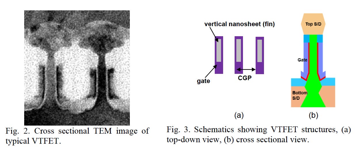
Unlike the rest of the industry, IBM has looked towards a different approach, with a different transistor architecture, one using vertical nanosheets. This architecture is known as the Vertical Transport FET (VTFET).
One advantage of this approach is that it allows the CGP to shrink more. The scaling of the CGP past 40nm with regular transistor architectures will prove to be extremely difficult and may come with too many tradeoffs in terms of resistance and capacitance. IBM previously presented on VTFETs at IEDM in 2021.
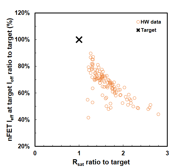
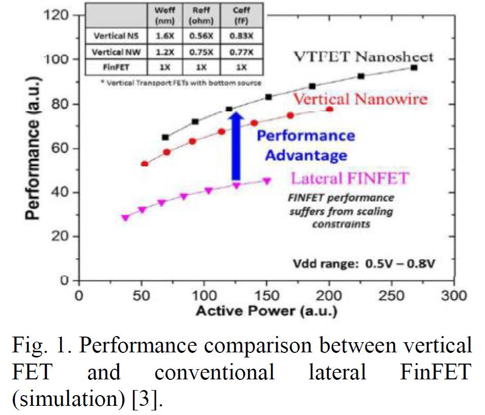
This time they showed VTFETs with a CGP of 40nm, using double diffusion breaks. They also stated that a zero diffusion break design is possible. Although IBM was able to fabricate such VTFETs, they found the capacitance was 20% higher than in simulations and the drive current was less than expected, with the best die at 90% of the target.
IBM showed off impressive performance improvements vs vertical nanowire by moving to this architecture.
Heterogeneous L-shaped Field Effect Transistor (LFET) for Angstrom Technology Nodes - Paper 20.2
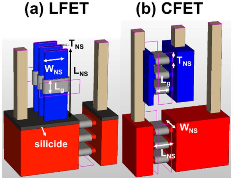
Several Taiwanese universities presented on a new transistor architecture, the LFET. This is, in some ways, a combination of IBM’s VTFETs as well as CFETs. The pFET is orientated vertically stacked on top of a horizontally orientated nFET. The “L” in LFET does not stand for anything is just the shape that this structure resembles. LFETs provide lower improvements in density, but they are easier to implement, and more easily adjustable. Contacts to the gates can also be formed much more easily.
These devices were simulated with 3 PMOS and 3 NMOS nanosheets. LFETs had slightly higher voltage droop. However, they also had lower power consumption and lower resistance.
Advanced Logic Technology — Metal Stack Interconnect
The scaling of the metal stack is crucial in every chip design as it is often the limiting factor. However, recent advancements in technology have hindered the scaling of the metal stack. When a current is passed through a metal interconnect, it creates heat and causes a flow of metal atoms, known as electromigration. This flow over time can cause voids and hillocks, resulting in device resistance increasing, and, eventually, failure.
The shrinking dimensions of copper interconnect amplifies this problem as the current density increases, causing greater heat generation and electromigration as well as more power loss in interconnects vs transistor switching. To address this, Tantalum Nitride barriers have been introduced, but as the interconnects continue to shrink, the barriers, being smaller in size, form a larger proportion of the lower metal layers, impeding the scaling efforts.
In Intel’s 10nm and Intel 7 nodes, cobalt was used for the lowest levels of the metal stack, though this has been walked back with Intel 4. Ruthenium was also used in their 10nm and 7nm nodes and is increasingly becoming the material that everyone hopes takes over.
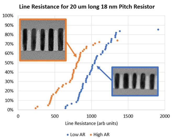
IBM Subtractive Ru Interconnect Enabled by Novel Patterning Solution for EUV Double Patterning and TopVia with Embedded Airgap Integration for Post Cu Interconnect Scaling - Paper 12.1
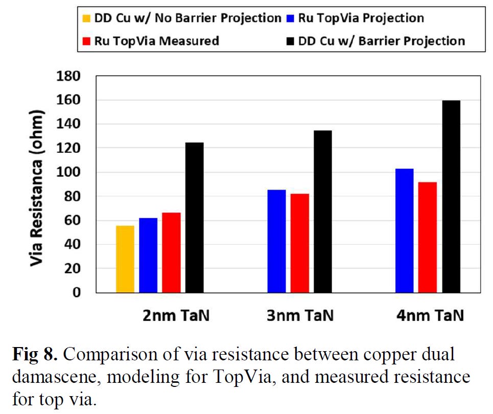
IBM Research and Samsung showed off their new interconnect using Ruthenium (Ru) instead of Cu. Ru, much like Cobalt, does not require a barrier and can scale to smaller widths, without gaining astronomical resistance and capacitance.
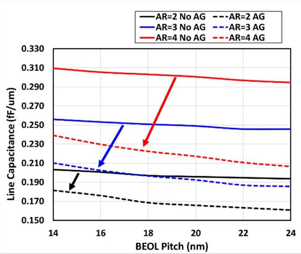
Although Ru interconnects can be fabricated with a dual-damascene process similar to copper, they used subtractive patterning for this new research. This required the use of spacer-assisted LELE (SALELE), with EUV. This allowed them to form interconnects with a metal pitch of 18nm, a 22% decrease from the MMP on TSMC’s N3E.
These also had a high aspect ratio of 4:1 which reduces resistance by 20%, at the cost of increasing capacitance. As SALELE builds the vias between metal layers on top of the interconnects, it is significantly easier to fill the space between the wires with air, which is the best dielectric available with a k=1. Compared to a low-k dielectric with k<2.7, this is a significant change that can reduce capacitance by over 30%.
Applied Materials Tungsten MOL Local Interconnect Innovation: Materials, Process & Systems Co-optimization for 3nm Node and Beyond - Paper 12.6
Applied Materials also showed off their new interconnects using Tungsten (W). Currently, Tungsten is deposited with Chemical Vapor Deposition (CVD), and has a barrier made of Titanium Nitride. Lam Research leads in market share with tungsten deposition due to 3D NAND, but Tokyo Electron and Applied Materials also operate. This new research showcases selective W, which does not require a liner. Current liners are usually TiN when using Tungsten.
If this technology is successful, it could be adopted in all advanced logic nodes, which would be a massive positive for Applied Materials.
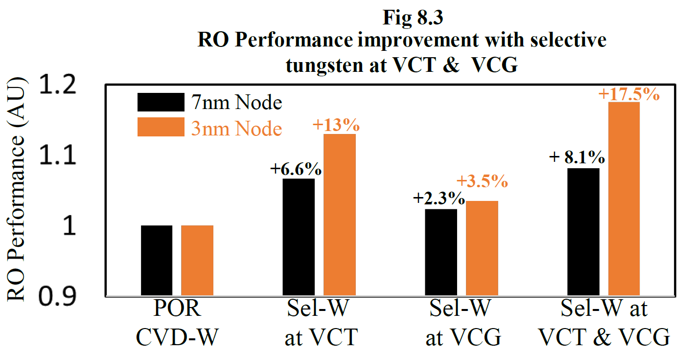
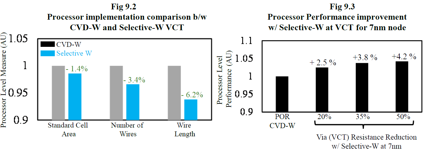
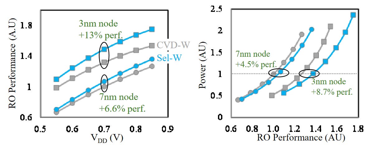
Much like Ru, this is a likely candidate to allow for future interconnect scaling. Through this new innovation, they were able to reduce the via and chain resistance by 40%.
They also showed that this process could result in as much as 13% higher performance at the same voltage, 8.7% higher performance at the same power and a 1.4% smaller standard cell area. Small innovations like this compound together to keep the wheel of semiconductor scaling turning.
This has huge potential for the signal-side interconnect on future devices with backside power delivery networks!
Advanced Logic Technology — Static Random Access Memory (SRAM)
Integration Design and Process of 3-D Heterogeneous 6T SRAM with Double Layer Transferred Ge/2Si CFET and IGZO Pass Gates for 42% Reduced Cell Size - Paper 20.5
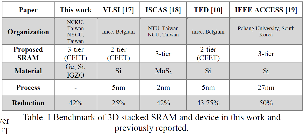
As TSMC’s N3E process shows, SRAM scaling has become incredibly difficult. While consistent gains will continue to be difficult to come by, SRAM has a few final tricks up its sleeve. Both the move to GAAFETs and CFETs should enable SRAM to shrink sizably, by 30-40% with each. Various Taiwanese universities showed a design for an SRAM bitcell with CFETs that used the area of just 2 transistors for a 6-transistor SRAM bitcell. They achieved this with sequential stacking.
With this, they were able to reduce the area by 42%. According to their research, the new bitcell design consumed 100 times less power at idle!
This is very interesting compared to other potential new designs for SRAM that move to the 3D realm, including from IMEC. Given the lack of SRAM shrinkage at TSMC’s N3E, this research is critical.
Advanced Packaging
We have previously written an overview of ECTC 2022, the premiere conference for advanced packaging. Nonetheless, TSMC, Intel and Samsung have provided updates to their advanced packaging technologies at IEDM. Advanced packaging is only becoming more important as the costs of leading-edge nodes increases ever further.
TSMC - Heterogeneous and Chiplet Integration Using Organic Interposer (CoWoS-R) - Paper 3.2
TSMC had some small updates on CoWoS-R. Although it was mostly reiterations of existing information, TSMC displayed they could package with an L/S of either 2μm/2μm or 1μm/1μm. They also showed it being used to link HBM3 to a chiplet.
Intel EMIB 3 - Paper 3.4
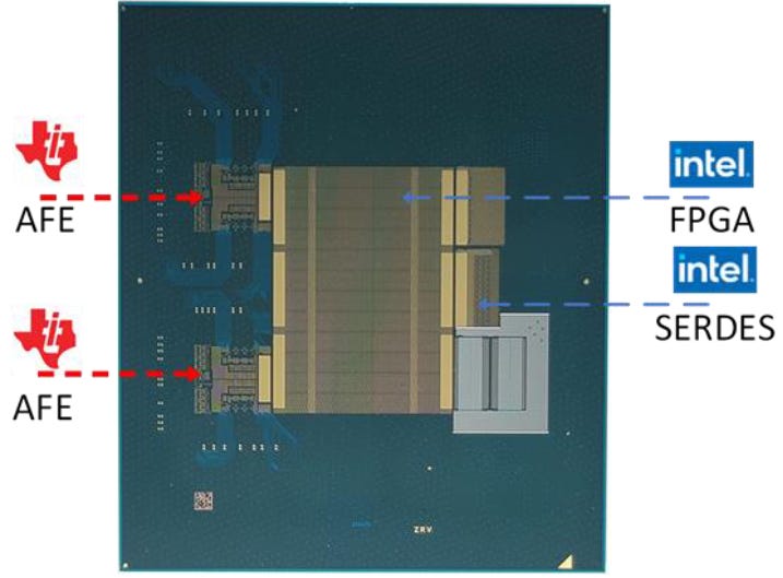
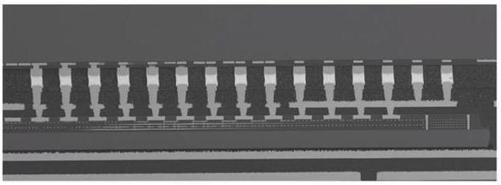
Intel presented on two of its packaging technologies, EMIB and Foveros Direct. With their 3rd generation of EMIB, EMIB significantly improved the accuracy of its placement, by over 3x. With the new process, the dies also move around 50% less when heated for the TCB process. They also showcased a package with an FPGA using AIB 2.0. The 3rd generation of EMIB with a 36 μm pitch was used to connect to an Analog Front End chip from Texas Instruments, under the DARPA CHIPS program. Based on the cross-section shown, the L/S seems to be 2μm/2μm, on par with their paper from ECTC in 2016. This an improvement over the 5μm/5μm L/S shipping in their products like Stratix 10 and Sapphire Rapids.
They also showed off a few yield improvement techniques in the actual paper.
Foveros Direct Reconstituted Wafer on Wafer Bonded - Paper 27.3
Intel’s 1st generation Foveros Direct has a pitch of 9μm, a 16x improvement in density over Foveros using microbumps. The 2nd generation will feature a pitch of 3μm, another 4x improvement in density. Of course, these are the minimum pitches, and as AMD’s 3D V-Cache Technology on Zen 3 shows, the minimum pitches are not always used. If Intel can stick to its roadmaps and deliver on its promises, it may be able to catch up to TSMC’s 4th generation SoIC, also with a pitch of 3μm.
According to Intel, the 2nd generation improves efficiency by about 20%. They also claim this will allow for near-monolithic designs with little to no power, area, and latency overheads. We find this hard to believe, but further scaling will help in these three areas. Finally, Intel also showed off some concepts for a system of chips using a mixture of many different packaging methods and stacked many layers high.

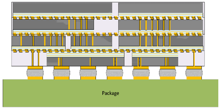
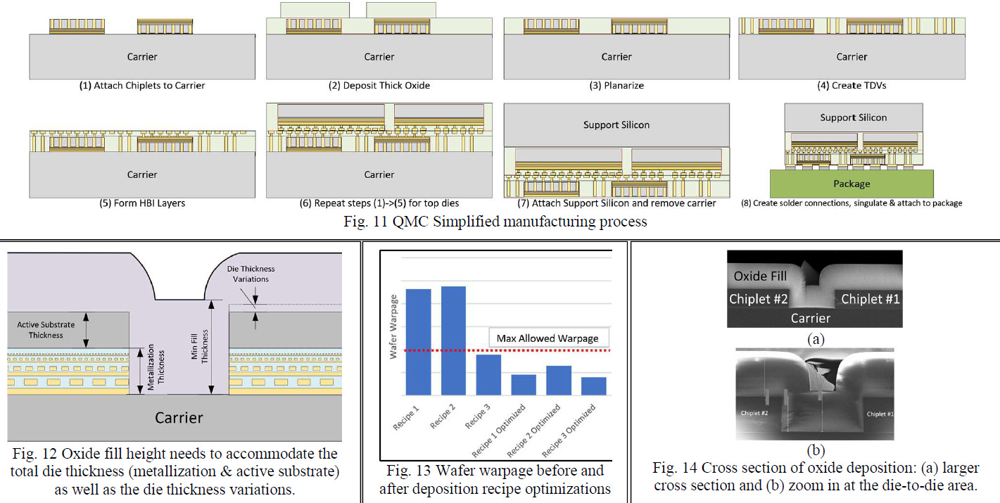
The most interesting thing about Intel’s process is that it is a reconstituted wafer on wafer bond.
They are branding it as quasi-monolithic chips (QMC).
Samsung Advanced Packaging, Hybrid Bond Logic 4um, Hybrid bond HBM - Paper 3.6
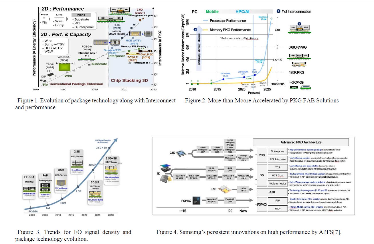
Samsung has remained behind in advanced packaging for some time now, and its packaging solutions have failed to gain major traction, although they are investing hugely to try to gain share. It’s X-Cube is planned to go into production in 2024 with microbumps, years behind TSMC and Intel, and with hybrid bonding in 2026, again years behind TSMC and Intel. Their packaging solutions are branded under the Advanced Packaging Fab Solutions (APFS).
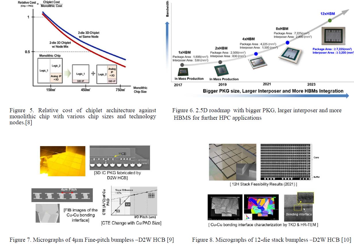
I-Cube is Samsung’s silicon interposer technology, similar to CoWoS-S. The 4th generation supports 8 HBM packages and 3x reticle size, about 1 year after TSMC. The next generation is said to support 12 HBM packages and 4x reticle size. Samsung also showed 12Hi HBM with hybrid bonding, which they achieved in 2021. Reminder, SK Hynix showed 16Hi HBM with hybrid bonding publically in 2021.
We expect Baidu to remain the only large customer using these, although this could be blocked by US Sanctions. Samsung’s X-Cube with hybrid bonding was shown to have a 4μm pitch, which could significantly close the gap if in production by 2026. However, there is a high likelihood it is only in production at a later date.
Unimicron Hybrid Substrates for Chiplet Design and Heterogeneous Integration Packaging - Paper 3.5
Unimicron also showed off some advanced packaging. They used a 55μm microbump pitch with both PID and ABF substrate and compared them. They showed off a 3 metal layer design with different pitches and line/space for each, as low as 3μm and 2/2μm, respectively. Although this packaging isn’t that advanced compared to those in HVM by TSMC or Intel, it still shows that OSATs are working on their own solutions.
Unimicron is a substrate supplier to Intel, AMD, and many others. We covered this specific paper in more detail here.
ASE Advanced Packaging Technology Platforms for Chiplets and Heterogeneous Integration - Paper 3.3
In recent years, ASE has been improving its portfolio of packaging options in order to stay competitive against TSMC and other companies. At IEDM, they provided a summary of many of their packaging options. Fanout Chip on Substrate (FOCoS) comes in many forms such as FOCoS-Chip First (FOCoS-CF) and FOCoS-Chip Last (FOCoS-CL). The difference between these is similar to TSMC’s distinction between CoWoS and InFO.
FOCoS-CF supports 4 redistribution layers (RDL) with line/space of 2/2μm. They showed a test vehicle with two 30x28mm2 dies on a 47.5x47.5mm2 package. FOCoS-CL features 4 layers of RDL with the same line/spacing. It features a microbump pitch of 55μm, similar to that of EMIB shipping in Intel’s Sapphire Rapids. The test vehicle shown had an ASIC die of size 30x28mm2, and two HBM stacks on a 47.5x47.5mm2 package.
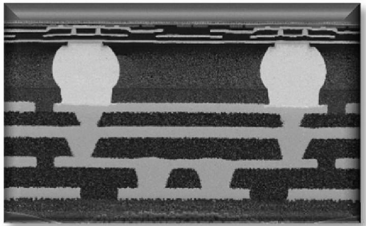

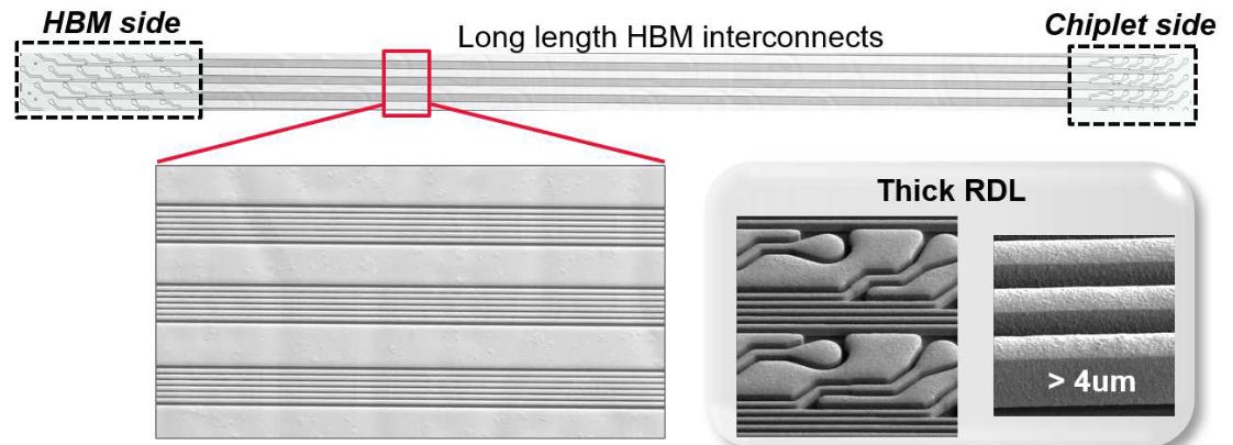
ASE also showed off FOCoS-Bridge (FOCoS-B). This involves the use of an embedded silicon bridge and has a line/space as small as <0.8/0.8μm. Their website states that it goes down to 0.6/0.6μm. We believe that FoCoS-B is a renamed version of the FOEB that SPIL developed before their acquisition by ASE. Their test vehicle showed FoCoS-B with a 0.8/0.8μm line/space. It had 2 ASIC dies and 8 HBM2e stacks.
We also have some further information on FoCoS-B/FOEB and one of its major customers.
We also want briefly discuss some yield issues AMD had.


