Intel Emerald Rapids Backtracks on Chiplets – Design, Performance & Cost
Competitive Analysis Considerations, Sapphire Rapids Stealthy Redesign
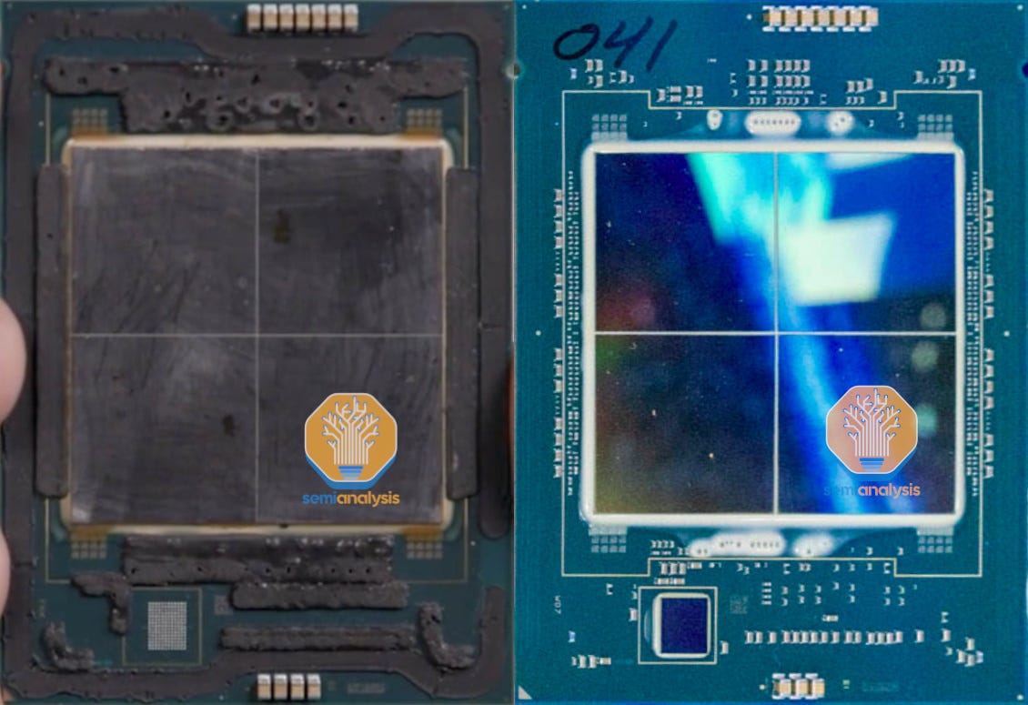
At Intel’s recent DCAI Webinar, EVP Sandra Rivera revealed what Emerald Rapids, Intel’s 5th Generation Xeon Scalable Processors, would look like under the lid. Intel has decided to backtrack on chiplets for a generation by designing Emerald Rapids (EMR) using just 2 large dies. Its predecessor, Sapphire Rapids (SPR), had 4 smaller dies. Counterintuitively, Intel reduced the number of chiplets in their highest core count configuration from 4 to 2. This would make most scratch their heads, as everyone, including Intel, has been talking up chiplet disaggregation with smaller dies to improve yields and scale performance.
Today, we want to dive much deeper into the specific changes Intel has made with Emerald Rapids (EMR) over Sapphire Rapids (SPR). We will be going through the floor plan diagrams that we created, detailed by workload performance, cost comparisons, and competitive environment versus AMD. Furthermore, we will be detailing a huge change that happened with Sapphire Rapids that slipped under most folks noses.
Emerald Rapids Changes
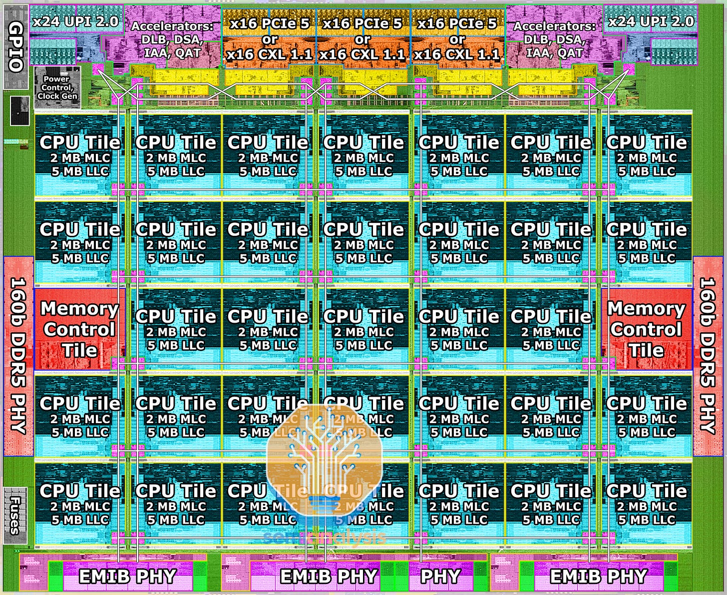
The largest variant EMR-XCC, bumps core counts to 64 from 60 on SPR. However, there are a total of 66 physical cores on the package, binned down to assist yields. Intel is not planning to productize a fully enabled 66-core EMR SKU like they did with 60-core SPR. EMR combines two 33-core dies, whereas SPR used four 15-core dies.
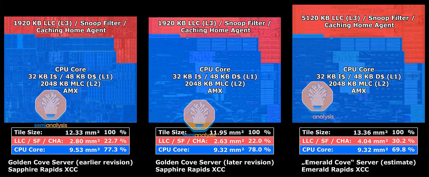
The other major change is that Intel dramatically increased shared L3 cache, from 1.875MB per core on SPR up to a whopping 5MB per core on EMR! That means a top-end SKU comes with 320MB of shared L3 cache across all cores, 2.84x the maximum that SPR offers. Local Snoop Filters and Remote Snoop Filters have also increased accordingly to accommodate the large L3 cache increase (LSF – 3.75MB/core, RSF – 1MB/core).
DDR5 Memory support has been increased to 5600 MT/s from 4800. UPI speeds for inter-socket communications have been upgraded from 16 GT/s to 20 GT/s. Oddly, despite higher inter-socket speeds, the number of total sockets supported is down from 8 to 2. This was likely done to speed time to market as it only affects a tiny portion of the market that AMD doesn’t compete in anyways. All this is drop-in compatible with existing “Eagle Stream” platforms on the same LGA 4677 Socket E1. PCIe lane counts remain the same, although CXL bifurcation support is added finally, which was a sore spot for Sapphire Rapids.
Taking a closer look at the package, we notice that Intel was able to cram more cores and a whole lot more cache into an even smaller area than SPR! Including scribe lines, two 763.03 mm² dies make a total of 1,526.05 mm², whereas SPR used four 393.88 mm² dies, totaling 1,575.52 mm². EMR is 3.14% smaller but with 10% more printed cores and 2.84x the L3 cache. This impressive feat was achieved in part by reducing the number of chiplets, which we will explain shortly. However, there are other factors at play that help with EMR’s area reduction.
While drafting floorplan mockups for EMR, we found it impossible to cram the necessary features into a small enough area to match what was revealed by Intel. We were using components from SPR as a reference, which ended up being too large. This is because Intel has optimized its physical design to make some features more compact and area efficient to achieve further area reductions. What’s more, this is not the first time Intel has changed physical design to save area.
Sapphire Rapids Die Shrink
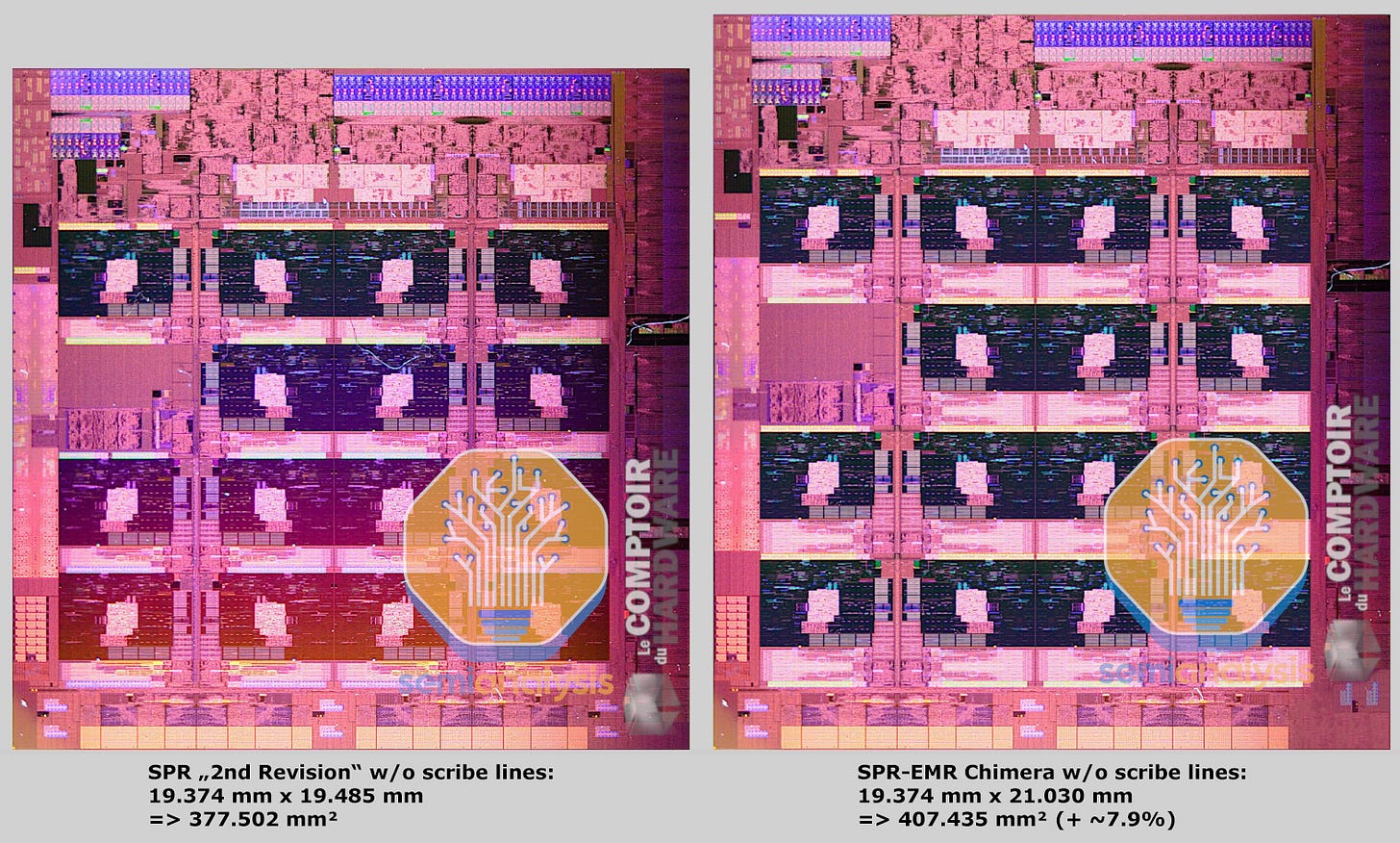
Although not discussed much publicly, Intel also did a complete ground-up re-design of Sapphire Rapids during its darkest days on its way to production E5 stepping. Believe it or not, there are two different physical designs and die sizes for the Sapphire Rapids chiplets.
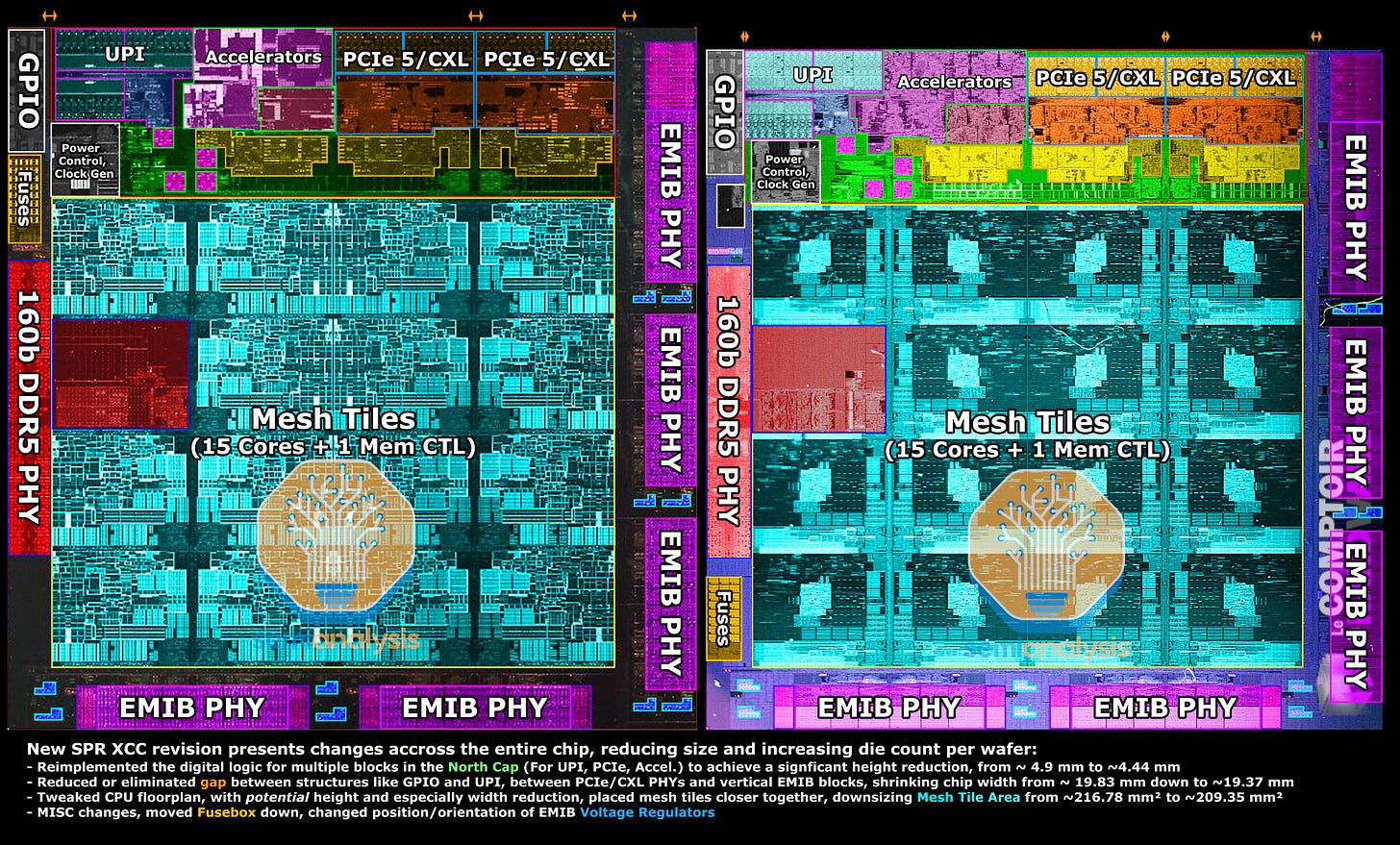
Raja Koduri showed the larger, earlier version of SPR at Architecture Day 2021, and is also featured in 3rd party teardowns of early engineering samples. The smaller, newer variant of SPR was shown at Vision 2022, which is used by the final production SKUs.
Intel has shown the wafers for both versions of SPR. The earlier revision had 137 gross dies per wafer while the final version had 148. This required going all the way back to the floor planning and physical design of the chip. One major benefit is that it improved the cost structure of Sapphire Rapids by manufacturing 8% more dies per wafer.
In the numerous silicon revisions done during SPR’s prolonged bring up, we identified that Intel changed the physical design and layout of the cores and periphery to achieve a 5.7% area reduction. The I/O area (North Cap) has been reimplemented to save 0.46 mm in die height. The horizontal spacing between I/O blocks has also been optimized, saving 0.46 mm in die width. The mesh tile area that houses the CPU cores, caches, and memory controller also had to shrink by 3.43% in area to fit in the tighter floorplan, with tweaks reduce to the CPU core width and tile spacing.
In general, it is quite uncommon for design teams to make 2 different layouts and die sizes of the same product before launch, as time to market is paramount. Perhaps the many delays to Sapphire Rapids gave them enough time to pursue additional area savings. If it launched on the original 2021 target, we likely would not have seen this smaller revision, at least initially.
In a similar vein, Intel applied the same principles of layout optimization for EMR, particularly in accommodating the huge L3. Here, we show a mockup of changes to the core and mesh tile, including a significantly taller SRAM section above the core to house the additional L3 cache and Snoop Filters. With this, the area of each core tile has increased by 11.8%. Thanks to optimizations in SRAM physical design, Intel were able to fit 3200 KB more L3 cache along with a larger LSF and doubled RSF by adding just 1.41 mm².
Emerald Rapids Floorplan
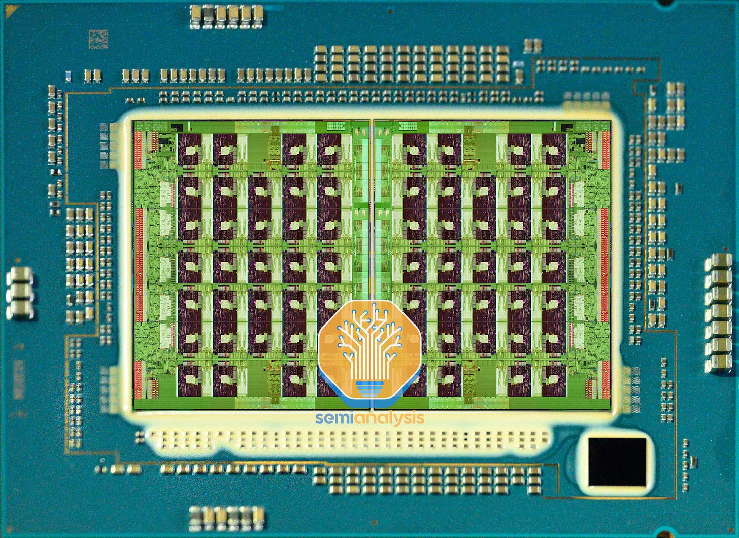
Below is the floorplan layout for EMR-XCC. Across both dies, the 66-cores plus I/O sections are lashed together on a 7x14 mesh interconnect network.
In the middle, the mesh network crosses the off-chip boundary 7 times over EMIB. This compares with the 8x12 mesh across four dies on SPR with 20 off-chip crossings. The implications of this topology change will be covered in the performance section below.
From the layout shown above, we show that despite how similar the two chiplets are, they are in fact using different tape outs and mask sets, with Intel once again going with mirrored dies as was done with SPR. Using the same die rotated 180 degrees would halve the mask set requirements but complicate their Multi Die Fabric IO across EMIB.
Speaking of EMIB, the number of silicon bridges has gone down considerably from 10 to just 3, with the middle one being wider to fit 3 mesh columns. The odd number of mesh columns is also featured on the monolithic version of SPR, and could also be part of why they had to mirror the dies, as a rotation would mess with alignment and complicate wire crossings.
With this new layout, we can see the true benefits of chiplet reaggregation. The percentage of total area used for the chiplet interface went from 16.2% of total die area on SPR to just 5.8% on EMR. Alternatively, we can look at core area utilization I.E. how much of the total die area is used for the compute cores and caches. That goes up from a low 50.67% on SPR to a much better 62.65% on EMR. Part of this gain is also from less physical IO on EMR, as SPR has more PCIe lanes that are only enabled on the single socket workstation segment.
If your yields are good, why waste area on redundant IO and chiplet interconnects when you can just use fewer, larger dies? Intel’s storied 10nm process has come a long way from its pathetic start in 2017 and is now yielding quite well in its rebranded Intel 7 form.
Cost – Not What You Think
All this talk about layout optimization and cramming more cores and cache in a smaller total silicon area would have you believe that EMR is cheaper to make than SPR. That is not the case.
Fundamentally, big rectangles just don’t fit neatly on a circular wafer. Going back to gross dies per wafer, we estimate that the EMR-XCC wafer layout matches SPR-MCC, meaning 68 dies per wafer. Assuming perfect yield and die salvageability, EMR could only do 34 CPUs per wafer, down from 37 CPUs per SPR wafer. It gets worse for EMR once factoring anything other than perfect yields, showing the disadvantage of going with larger dies.
Despite using less silicon area per CPU, EMR actually costs more than SPR to produce.
In fairness, if we were to isolate the benefit of the layout changes to cost, we should be comparing EMR to a hypothetical SPR with 5MB L3 per core. Area estimations from this taller, theoretical die lead to 136 gross dies per wafer or 34 CPUs per wafer for this 4-chiplet variant, making it identical to the actual 2-chiplet design. Furthermore, reducing the number of EMIB dies from 10 to 3 would definitely improve packaging costs and yields for the 2-chiplet solution.
So, if the layout changes and chiplet reduction didn’t help with cost, then what is the primary driving factor for EMR?


