Intel’s 14A Magic Bullet: Directed Self-Assembly (DSA)
How High-NA EUV can be economically viable at the 1.4nm process node
Intel’s 18A node gets most of the spotlight recently – with an ongoing battle between TSMC’s and Intel’s management teams on the merits of TSMC N2 vs Intel’s 18A. However, it is 14A that will be the make-or-break node for Intel Foundry. Winning customers starts with process technology, and Intel is betting big here, but they need a generation where everyone gets comfortable. Customers will use 18A to dip their toes in the Intel waters with less critical chips that are not core to their business; if all goes well, they will look to 14A as the main process for their linchpin designs – think the largest, expensive dies like AI accelerators, CPUS, and potentially even mobile in 2027.
Intel will need to win their business to make its IDM 2.0 foundry strategy work, or else they will not have enough scale and volume to compete given their internal product business will continue to lose market share for the next few years. It simply isn’t possible to run a leading-edge foundry without multiple large, leading-edge customers.
Intel will be the first, by a margin of years, to adopt ASML’s high-NA EUV lithography scanners in high volume manufacturing. Both TSMC and Samsung have only ordered tools for R&D. Intel, perhaps trying to correct for being late to the low-NA game, has been high-NA’s loudest and strongest champion. With the first customer-owned example now being installed in their Hillsboro fab, Intel will have a head start on R&D and real-world experience with high-NA scanners.
But there is the question of economics. Our model shows that high-NA single exposure is more expensive than low-NA double patterning.
And other chipmakers have publicly signaled that high-NA is too expensive through both their low orders and with public commentary:
Technology itself is of no value. Only what can serve your customer. So we always work with our customers to give them the best transistor technology and the best power-efficient technology and at a reasonable cost, okay? And more importantly, the technology maturity that -- in the high-volume production, that's all important. Everything. Everything counted together. So we -- every time we know that there are some new structure, new tools such as high-NA EUV, we look at it carefully, look at the maturity of the tools, look at the cost of the tools and look at the schedule of that -- how to achieve it. We always make the right decision at the right moment to serve our customer.
C.C. Wei, TSMC Vice Chairman & CEO
Why, then, would Intel Foundry bet its future on high-NA if it is more expensive? At SPIE Lithography and Advanced Patterning, and now more recently with Intel’s new announcement, we finally heard the answer: directed-self assembly (DSA), Intel’s magic bullet that dramatically lowers lithography costs.
Below we’ll discuss what DSA is, how it could potentially make high-NA economical, go through the technical details of how DSA works, and the risks involved with adopting this new technology. We’ll also show an updated cost model including high-NA + DSA, talk through the potential applications beyond critical layers on leading-edge logic, and finish with the implications for the companies involved – Intel, TSMC, the single source DSA materials supplier who could benefit, ASML future outlook with tool orders which is quite non-consensus from the drama of yesterday’s earnings, and more on 14A challenges.
Why Directed Self Assembly Is Needed: Breaking the Dose vs. CD Tradeoff
The main challenge driving high cost on high-NA is the critical dimension (CD) vs. dose curve and its flow-through to throughput and cost per wafer. Critical dimension is the width of the smallest line or space that can be imaged by a lithography scanner. Achieving good image quality at lower CDs requires exponentially higher doses. Because of limited light source power, delivering higher doses means the scanner must run more slowly, waiting for enough photons to reach each exposure field. Running slowly means fewer wafers produced by the scanner, which translates to a big cost increase when using a tool depreciating by more than $150,000 per day. For a more detailed discussion, see our piece on high-NA cost.
Lower exposure doses allow the scanner to run at or close to its maximum, stage-limited throughput. While normally the image quality would be unacceptably poor, with directed self assembly it can be rectified. Directed Self Assembly (DSA) is a nanopatterning technique that utilizes the self-organizing properties of block copolymers, guided by pre-patterned templates. In simple terms, it can repair the feature, dramatically reducing the dose required and actually improving the final pattern quality.
How Directed Self Assembly (DSA) Works
The mechanism of DSA is there in the name: a chemical that is “self-assembling” and does so in the location where it is “directed.”
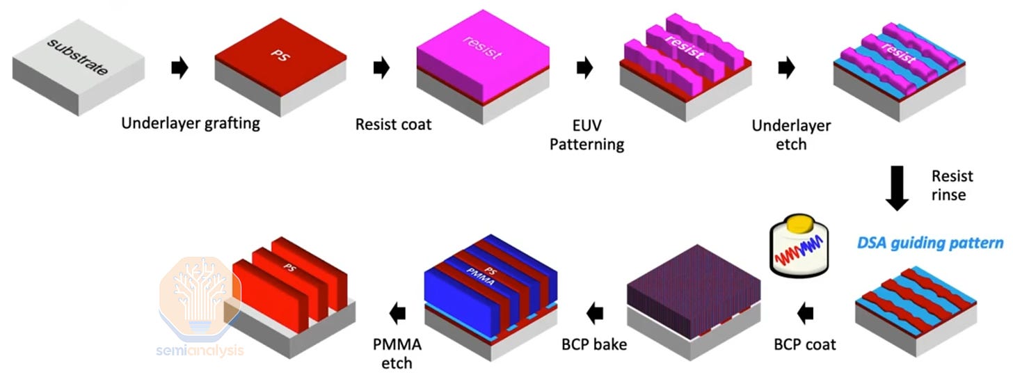
“Self-assembly,” despite the complex chemistry behind it, is an intuitive concept – components that start off randomly arranged organize into a useful structure when energy is added to the system. Imagine (this is slightly hyperbolic) a Lego set that builds itself when you bake it in an oven.

Chemically, this behavior is achieved with a block co-polymer (BCP). Two polymers, only a handful to dozen nanometers long, are linked by a covalent bond to form the BCP. The current state-of-the-art polymer used is polystyrene-block-poly(methyl methacrylate), abbreviated as PS-b-PMMA.
The two polymers, PS and PMMA, do not mix well. Just like oil and water, PS is a nonpolar molecule while PMMA is polar – they naturally will separate into layers, as that’s the lowest energy arrangement. PS-b-PMMA, naturally wants to arrange into a regular, orderly pattern of layers. Adding energy in the form of heat allows the molecules to more quickly find this equilibrium arrangement.
In practice, this means coating a wafer with PS-b-PMMA and baking it for less than an hour results in a regular pattern of PS and PMMA alternating lines, each ~20nm wide. If that sounds like a good starting point for producing ultra-thin metal wires to connect billions of transistors together (an M0 layer in leading-edge logic)... you’d be correct.
But this method of self-assembly alone is pretty useless, since the placement and orientation of the lines is more or less random. It needs to be guided, and that’s where lithography comes in.
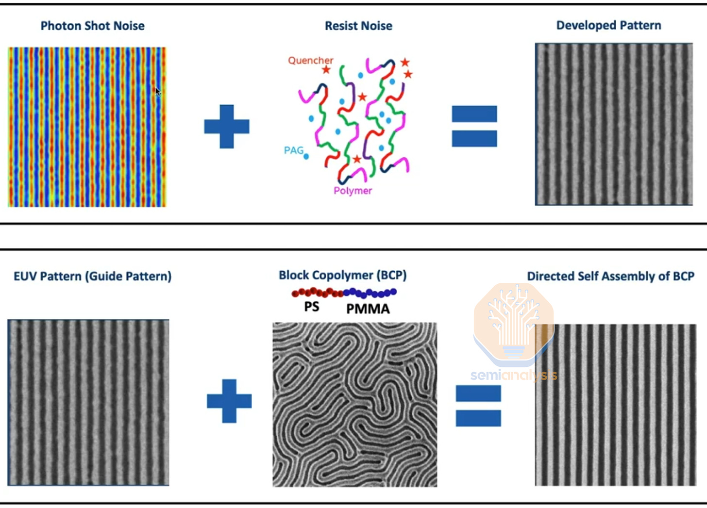
An EUV exposure is used to produce the guide pattern: this defines the orientation and position of the self-assembly. The process is very similar to a normal EUV lithography flow, except the pattern is transferred from photoresist to a special underlayer customized for DSA. This underlayer has a chemical affinity for only one of the block copolymers. With this patterned underlayer, during the bake the copolymers will not only align relative to each other but also relative to the underlayer – so the line placement is exactly where desired.
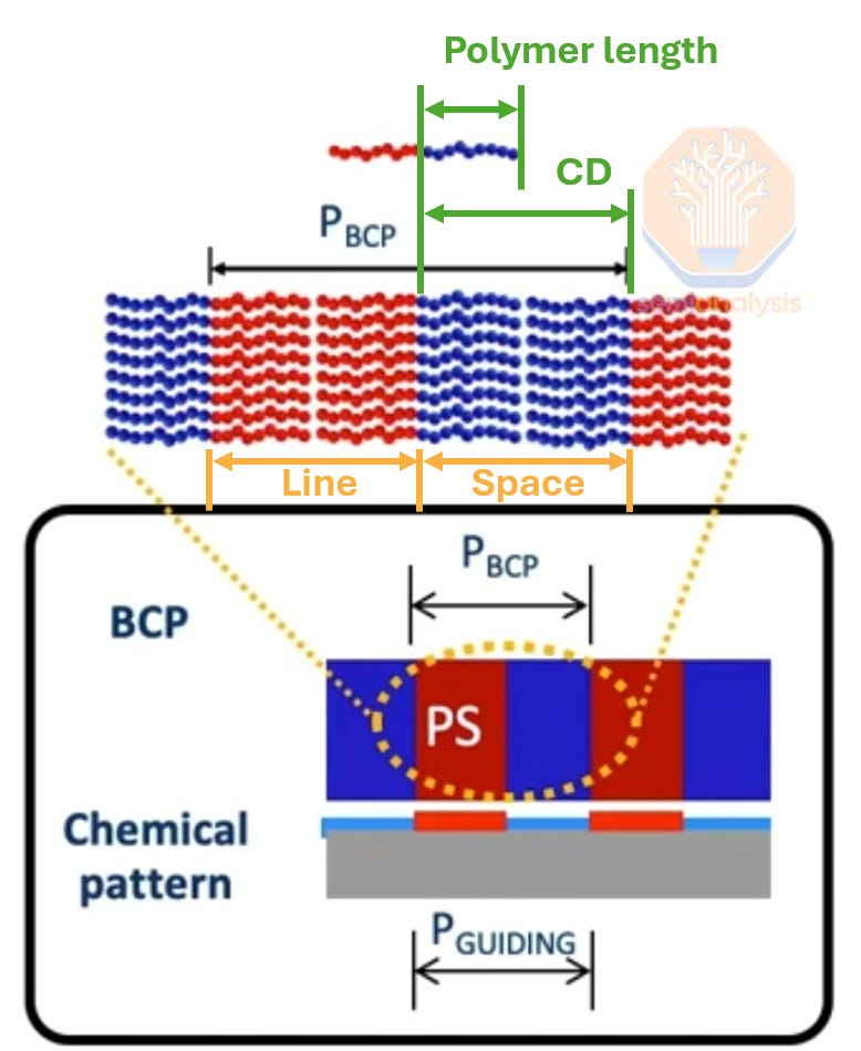
The critical dimension of these lines is defined by the length of each polymer chain. This means the BCP can be customized to print features as small (or large) as the polymer chains can be produced. The leading manufacturer of DSA chemicals in this application, has shown a 9nm CD with the possibility to go smaller. This is good enough to compliment high-NA EUV.
And here’s the key detail for the EUV-produced guide pattern: it can be produced with much lower doses. The DSA molecules self-assemble into lines with very low line edge roughness (LER), regardless of the LER of the guide pattern. They will align with the average of the guide pattern. As long as the guide pattern is placed accurately (which it can be, EUV overlay is very good), the LER of the EUV exposure can be poor – DSA can heal it. Relaxing image quality requirements for the EUV exposure means the dose can be reduced by 50% or more.

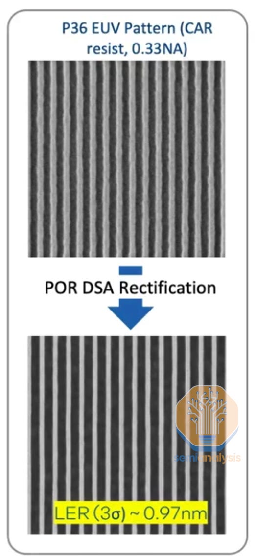
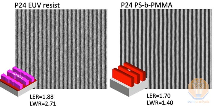
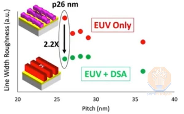
We use the 50% number for dose reduction as a reasonable assumption based on existing, replicated work. Early R&D work from Intel using a “novel underlayer” that can be patterned directly with EUV exposure, rather than by pattern transfer from photoresist, shows 25 mJ/cm2 dose is viable – a 3-4x reduction. If this is what can be brought to production, then the cost savings are much higher than even what we model below conservatively.
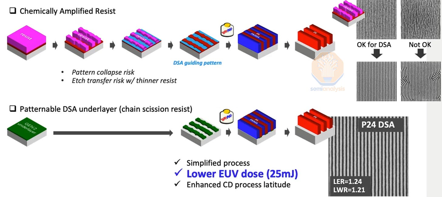
The final piece of the patterning puzzle is a dry etch: PS-b-PMMA can be selectively etched so just the polar molecule (PMMA) is removed. PS becomes the line, PMMA leaves the space – it ends up acting more or less the same as developed photoresist, so the typical post-develop integration flows (pattern transfer to hardmask, SOC, substrate, etc.) can be used.
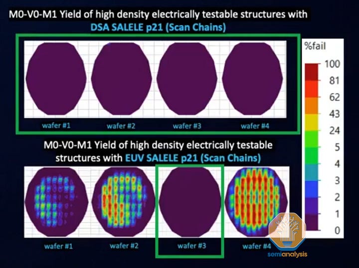
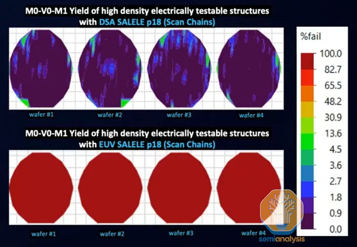
Ultimately the experimental results speak for themselves. Intel showed exceptional yield results for a self-aligned EUV litho-etch-litho-etch scheme when using DSA to rectify the pattern:
What’s the Catch? (Risks)
So far this is a near-perfect story for DSA. Given the product described above, every chipmaker would be using it for every EUV layer. But at the moment they are not. It’s been stuck in research for well over a decade. Why?
Below we’ll discuss the risks Intel has with adopting this new technology. We’ll also show an updated cost model including high-NA + DSA, talk through the potential applications beyond just critical layers on leading-edge logic, and finish with the implications for the companies involved – Intel, TSMC, the single source DSA materials supplier who could benefit, ASML future outlook with tool orders which is quite non-consensus from the drama of yesterday, and more on 14A challenges.


