Is Ampere Computing’s Cloud Native Marketing Fluff? – Siryn Ampere One 5nm Architecture, Cost Analysis, and IPO Analysis
In this article, we will discuss Ampere Computing and their “Cloud Native” CPUs. SemiAnalysis always gets asked if this is just marketing fluff or if there is something meaningful behind those words, so consider this an explanation of the merits and deficiencies. We will be doing a cost comparison of the current generation Ampere Altra and Altra Max versus Intel’s Ice Lake, and AMD’s Milan server platforms. We will also speculate on how the next generation of Ampere One, Intel Sapphire Rapids, and AMD Genoa could potentially shape out in the cost department. We will discuss our thoughts on the upcoming IPO.
Lastly, we also will discuss their 5nm based custom Ampere One architecture which will be coming on the server chip codenamed “Siryn”. While we do not know performance of these next generation CPUs, there is quite a bit of data that we be obtained through GitHub LLVM code. With the help of Cardyak, we were able to dig through and determine some of these architecture details. We have even created architecture diagrams that can be compared to other Arm based cores. There is also a YouTube video for those of you who prefer to watch and listen rather than read.
Cloud Native – Is it Marketing Fluff?
Ampere Computing was quite scant with details in their annual roadmap and strategy update, so we want to explain the base trend around their products. Ampere boils down their overarching strategy boil it down to 2 words, “Cloud Native.” AMD and Intel must target their CPUs for a wide range of workloads ranging from various flavors of enterprise and cloud. These range from storage servers to web servers to accelerator-based AI systems. These AMD and Intel CPU cores also go into client computing applications with only a few modifications. Ampere claims they can laser focus on the fastest growing segment of the datacenter, cloud, and optimize their product for it. They believe the future of computing will rely heavily on microservices, containerization, and serverless execution models. These concepts are generally about scaling performance out via a large amount small jobs and processes and breaking the bounds of single threaded CPU performance. Ampere gives 3 main ways their CPUs are “cloud native.”
Higher performance per CPU
Predictable performance
Scalability
Let’s break down how their architecture achieves this. Ampere Computing realizes their higher performance by having higher core counts. These higher core counts are achieved by utilizing smaller cores versus Intel and AMD. Ampere Computing cores are behind AMD and Intel in the area of single threaded performance, especially in floating point performance. The cores are by no means weak, but many workloads do rely heavily on single threaded performance which Intel and AMD offer at the cost of higher transistor counts and silicon area per core.
Ampere computing also offers more predictable performance by running only 1 thread per core. Intel and AMD offer 2 threads per core, simultaneous multithreading (SMT), which can cause unpredictable performance. Ampere Computing also believes that eschewing SMT allows their CPUs to be more scalable and secure. Exploiting vulnerabilities in SMT is a common method of side-channel attacks which have exploded in popularity since the advent of Spectre and Meltdown. SMT is not a pure negative. It takes advantage of gaps in workloads primarily caused by waiting for memory and allows the execution resources of the hardware to utilized at a higher rate. SMT increases performance while barely increasing the silicon area and transistor count per core. This predictability of performance also extends to Ampere’s cache architecture. Each core has a larger private L2 cache, while the shared L3 cache is relatively tiny. AMD and Intel rely on larger shared L3 caches which help in many workloads, but can also hamper predictability of performance.
Ampere Computing also place large emphasis on maintaining clock speeds at a certain level rather than opportunistically boosting. Intel and AMD CPUs vary their core clock speed significantly based on how many cores or threads are in use, and what type of code is executing. This helps their CPUs maximize performance within a given power and thermal budget. This is a huge advantage in many workloads. Ampere Computing increases the predictability of performance by ignoring this and adhering to certain clock speeds, a decision they believe makes the most sense for “cloud native” CPUs.
The strategy of cloud native CPUs is being copied by Intel and AMD with their upcoming Sierra Forest and Bergamo product architectures. Both have been described as targeted at cloud workloads, but those platforms are not coming as soon as Ampere’s next generation is.
Cost Comparison
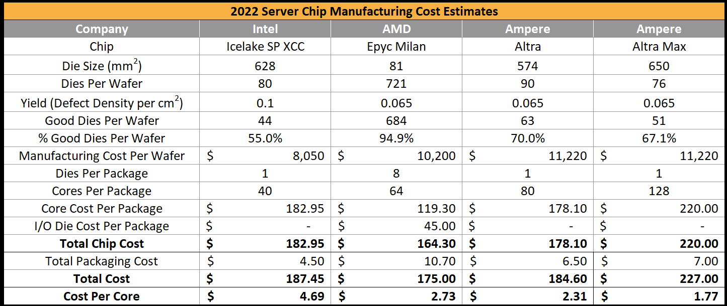
Overall, the smaller, simpler cores and the lack of technologies such as SMT and boost clocks reduce the design and validation timelines which allows Ampere Computing to reduce their design costs. For SemiAnalysis, the core size argument is the most important one. The 80 core Ampere Altra die has been estimated to be about ~574mm2 while the 128 core Altra Max has been estimated to be around ~650mm2. This is much less silicon than AMD’s 64 core Milan or Intel’s 40 core Ice Lake.
Let us demonstrate by comparing cost to manufacture. There are a lot of assumptions in the table below including wafer cost, yield, and the complete lack of acknowledging die harvesting. Die harvesting is when defective dies can still be sold by cutting down core counts or other capabilities. Parametric yield is also not accounted for. This is especially meaningful to Intel as they sell the largest dies and have the lower yield versus the TSMC process nodes that AMD and Ampere rely on. Intel also produces the smaller 28 core HCC die which is not shown. Advantages in binning related to chiplet implementations or more relaxed clock targets for various SKUs is also not accounted for. A 10% cost increase is assumed for wafer costs for Ampere vs AMD despite using the same node due to volume differences. Royalties to IP providers is also not accounted for. There are many fixed designs and tape out costs such as masks that are not contemplated. Take this as a demonstrative example, not a fact. We have done more advanced cost analysis with more accurate figures that take into account some of the above items, but that sort of model would take much longer to explain for this format. Lastly Server TCO is influenced by many other factors outside of pure CPU costs, so this is only a part of the puzzle.
Edit: The actual die size was revealed for Ampere Altra. We incorrectly estimated die size initially and have updated the table below with the correct figures.
The cost per core is lower for Ampere. It is nearly half the cost per core versus AMD and the discrepancy is even larger with Intel. This is an inherent advantage of the core architecture Ampere have chosen. Ampere does this through the combination of smaller cores, smaller L3 caches, and reducing fabric area by putting 2 DSUs per mesh stop, and 2 cores per DSU. The current generation uses the N1 core from Arm. Performance cannot be ignored, and the Ampere chip does not perform nearly as well in many benchmarks. With that said, when the workload represents many individual tasks that are not inter-related, Ampere often have much higher performance, even beating out AMD’s Milan CPUs. We recommend checking out this review from our friends over at ServeTheHome.
Roadmap And Current Success
Ampere Computing’s Siryn chip will be based on the custom Ampere One core architecture. It will also use DDR5 and PCIe5. The architecture is still monolithic and does not utilize chiplets.
Renee James had very interesting quote from the announcement of their next generation product.
We’re going to have two families of products. Our products coexist. They have features and performance for different workloads, market segments and application use. Like our 32 core 40 watt products for edge use.
Renee James, CEO and Co-founder of Ampere Computing – Source for quote
Despite all the hype about being cloud native, Ampere actually found another win in an unexpected place. GM’s Cruise autonomous driving unit is actually using an Ampere Altra variant that has 32 cores in a 40W envelope. This is quite odd, but the use case makes sense. Carl Jenkins, VP of Hardware Engineering at Cruise stated it is because they need to manage all the different sources of sensor data. Ampere’s Altra was the only CPU which had the level of CPU throughput required, but at a low power.
Customers can seamlessly move workloads between all of our Ampere processors. Also, we do not obsolete our roadmap when we offer a new product. In the consumer electronics business, the newer products obsolete the prior generation. That isn't the case with the Ampere cloud native roadmap. Ampere Altra 80 core and Altra Max 128 core are the mainstay of customer designs. In addition, the same customers are adding new Ampere One 5nm products for even further performance and feature evolution.
Renee James, CEO and Co-founder of Ampere Computing – Source for quote
This was a very odd quote to us. While server CPU lifecycles are longer, Intel is rapidly scaling down production of their previous generation Cascade Lake server CPUs as Ice Lake ramps, and AMD is rapidly scaling down production of their Rome server CPUs as Milan ramps. The same thing will happen to current generation platforms in 2023 and 2024 as Sapphire Rapids, Emerald Rapids, and various variants of AMD’s Zen 4 architecture such as Genoa and Bergamo ramp up.
We can only speculate on what she meant as Ampere did not respond when we reached out to ask, but it could be that their next generation product will scale to a higher cost and power envelope. It also could just be fluff around server CPU lifecycles and committing to shipping the current generation for a few more years so that they continue racking up wins.
These wins by the way are quite significant. Ampere is in almost every major public cloud, Microsoft Azure, Tencent Cloud, Alibaba Cloud, Oracle Cloud, and Equinix Metal. The major missing cloud is of course, Amazon. The exclusion of Ampere makes sense given Graviton 2 is quite similar to Ampere Altra from an architectural perspective, with both being based on the same Arm N1 core. While there are differences, it wouldn’t make sense to offer that hardware to their customers. As Ampere’s architecture diverges from what Amazon is working on, we would expect Amazon to begin offering Ampere based instances. Ampere has also had success with server manufacturers such as Gigabyte, Inspur, and SuperMicro. None of the sales volumes are disclosed yet, but we hear the vast majority of Ampere’s sales are to the public cloud vendors discussed above.
Ampere’s roadmap has an annual release cadence. This is in line with what AMD and Intel are doing. What isn’t inline with AMD and Intel is their design methodology. Or at least their claims about the design methodology.
One of the core tenants of how we’re actually doing our architecture and design – we have adopted much more of an agile software approach. The roadmap is more about having a constant cadence of releases; we have a bunch of features and then we find the right intercepts for them, and so the releases aren’t going to change, but over time, we can add and subtract features as we learn things based on customer feedback. With us, if you want to add a feature, 18 months later, it’s actually in and it doesn’t take three, four, or five years.
Jeff Wittich, Chief Product Officer of Ampere Computing – Source for quote
This claim is quite enormous. We have to imagine this is not directly related to core architecture, because that is simply too fast given CPU core and productization timelines. For example, we know of one such low level core architecture feature that Google requested of Intel 6 years ago, that will only come to market in 2023. While this example is most definitely due to Intel being in the process of catching up on roadmaps and implementing their new design methodology, even AMD would take 3 or 4 years or so for this level of a change. There could be a number of other features, especially related to IO, that this claim could be true in. AMD with their current chiplet style architecture, and Intel with their future tile-based architecture likely can implement these sorts of changes fairly rapidly.
Architecture
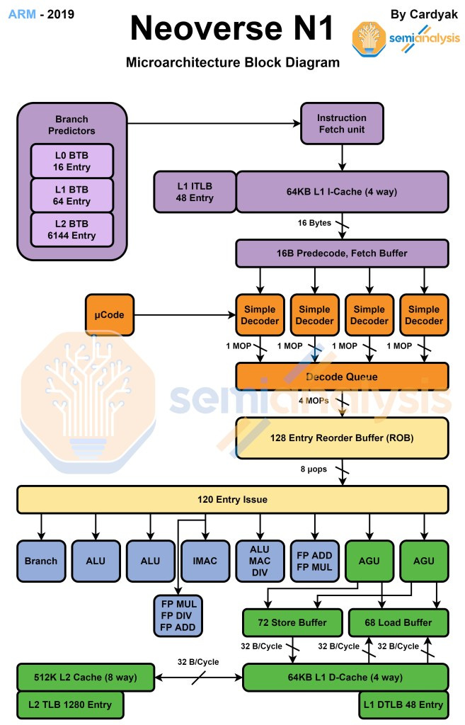
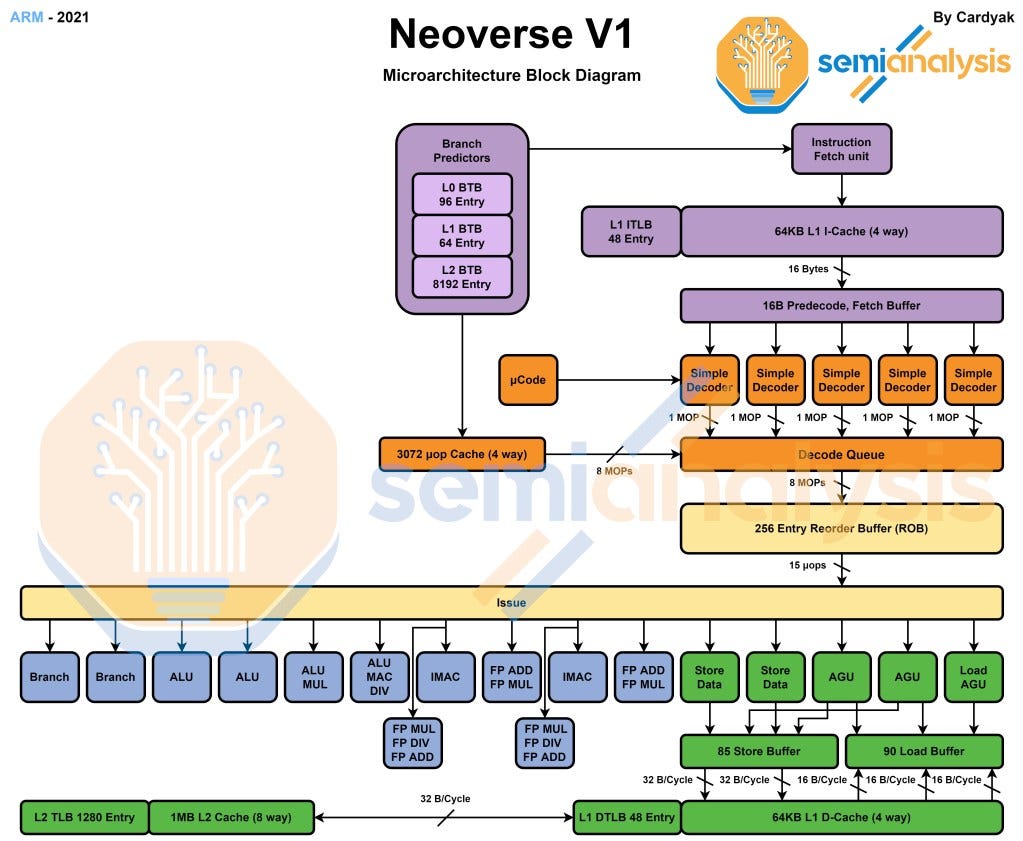
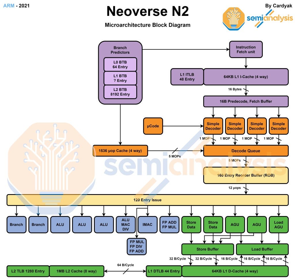
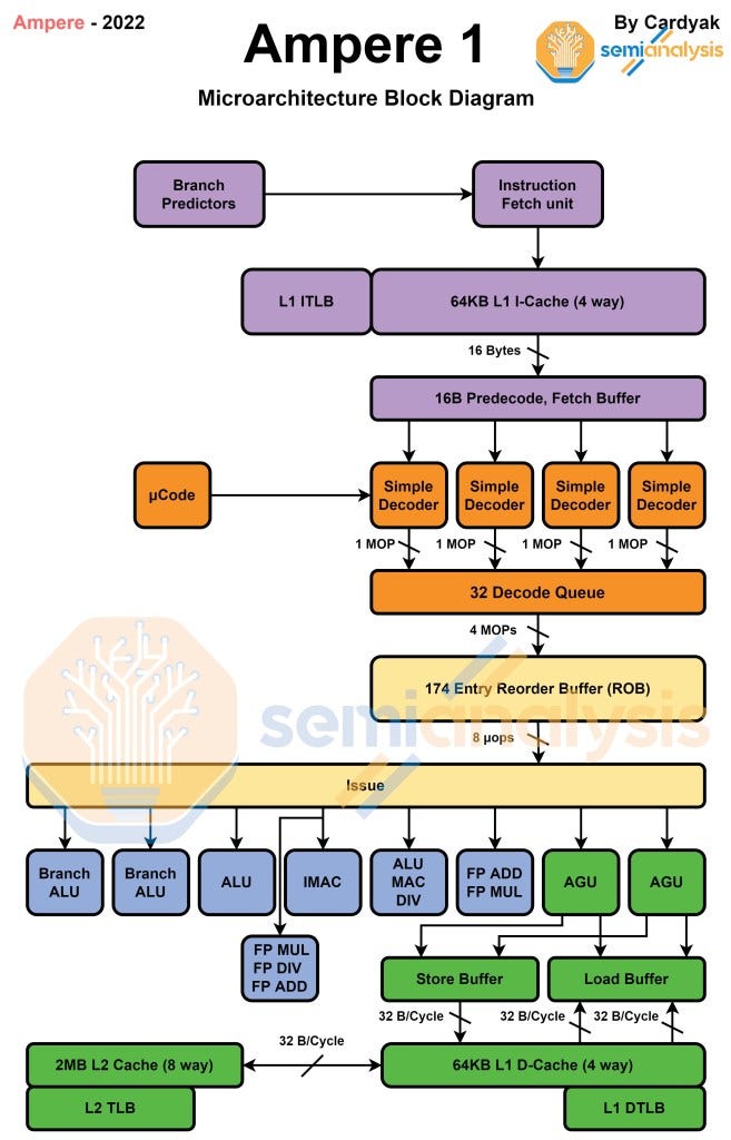
For those of you who like architecture, this section is for you. If not, skip down to after the table comparing the details. Cardyak created these diagrams at our request after we pointed out that details of the architecture could be found in LLVM code on GitHub.
Note: L2 cache is dynamic for the stock arm cores, but only 1 number is shown in the diagrams below for simplicities sake.
This is a very small core relative to what the x86 competitors use. Amazon Graviton 2, Ampere Altra, Ampere Altra Max, and Intel Mount Evans use this core. It is derived from Cortex A76 and implements the Armv8.2-A instruction set. Arm’s roadmap had a bit of a divergence for their next generation cores. The N line is continued, but they also offered the V1 core, which is much larger but has significantly higher performance per core. The peak floating-point performance is doubled and SVE is implemented. These changes bring single threaded performance in line with Intel and AMD’s current generation, but it also brings core size in line with them.
This V1 architecture is currently used in Amazon’s Graviton 3 chip. It will also be used by the European, South Korean, and Indian domestic HPC efforts. This core is most similar to the Cortex-X1 core, but it implements the Armv8.4-A instruction set.
Compared to the Cortex-X1, it features a deeper Reorder buffer to extract more instruction level parallelism (ILP) and can also execute 3 loads and 2 stores per cycle, compared to the Cortex-X1 with 2 loads and 1 store per cycle. It also features slightly larger L1 TLB sizes. There is a 3K Entry micro-op cache, which is very large, even bigger than Intel’s Sunny Cove and AMD’s Zen 3. V1 also adds support for new bFloat16 and Int8 data formats which are primarily used for processing AI and machine learning workloads. All the various changes mean that V1 is nearly 50% higher IPC versus N1.
Arm’s other next generation core is coming to the market soon is N2. This core is only 10% less performance than V1, but at significantly less area and fewer transistors. The peak floating-point performance is halved versus V1, but SVE2 is brought to market, which will help significantly in floating point workloads.
The N2 architecture is going to be much more common. Marvell has already announced multiple chips with this architecture. In addition, multiple hyperscalers are likely to implement this architecture. We know of at least 2 US based hyperscalers who have chips with this architecture in design. Lastly, there are 3 Chinese companies which claim to be bringing N2 based server chips to market as well. Two are Chinese hyperscalers, and one is an independent merchant silicon firm.
This core is most similar to the Cortex-A710 core. This core implements the Armv9.0-A instruction set, which brings a whole host of well publicized improvements. It offers a massive 40% more IPC versus N1. This required roughly 40% more transistors though. The core is about the same size on 5nm as it predecessor, N1, was on 7nm. The branch predictor can predict 2 taken branches per cycle, double that of N1 which can only predict 1 per cycle. N2 has a 1.5K Entry Micro-op cache which should reduce power consumption and increases IPC due to faster mis-predict recovery (at the expense of area). Rename width has increased from 4 to 5, and the backend now has 4 ALU's instead of 3 in the N1.
While many of the architecture related to Ampere One are missing, many are known. Ampere One implements Armv8.6, but it does have some features from Armv9.1. The width of the core appears to be very similar to N1. The core is definitely larger and higher performance though. Ampere doubled the L2 cache. They also appear to have 2 branch units as opposed to the 1 of ARM Neoverse N1. This core does not implement SVE in any form.
The most important detail about Ampere One is that it continues along the lines of their current “Cloud Native” strategy. It should be much smaller than what Arm partners will do with Neoverse V1 and Neoverse N2. The difference in core size between Ampere One and next generation platforms such as AMD Genoa and Intel Sapphire Rapids will grow substantially. We will discuss the comparison to these platforms with an ad-hoc cost comparison and discuss our thoughts on the IPO and future of merchant silicon in the subscriber only section.
Note that cost for Sapphire Rapids and Genoa will be far more accurate than the estimated Ampere one due to the complete lack of first party details beyond process node and scaped architecture details.


