The US Government is finally looking to pass CHIPS Act, well it has seemed that way for a year, but for real this time folks! Only issue with the passing is our lawmakers keep packing a bunch of other unpopular legislation alongside, whether Republican or Democrat. In the end they both agree on this, it’s just a matter of what pork they want to stuff into the bill. Lawmakers, think tanks, purchasing manager, and many others assure me it will pass this year and the subsidies will be in place.
If true, semiconductor equipment spending by firms in the US will likely be subsidized to the tune of a 40% tax credit. The logical conclusion to a subsidy of this sort is to spend as much of your capital expenditure in the US and as little as possible outside of the US. There also may be ways to play games with this subsidy though, and even potentially abuse it.
Intel is currently building out their Ireland Fab 34 as well as some US Fabs for their Intel 4 process node. This is an expensive undertaking, but one that will catch Intel up in process technology if all goes well. The tooling is incredibly expensive, not just from the expensive EUV and DUV lithography tools, but also for all the other associated equipment. Lithography tools will be roughly 20% of Intel’s spending in Ireland, but many other firms are also receiving orders. One such firm is the Japanese giant, Tokyo Electron.
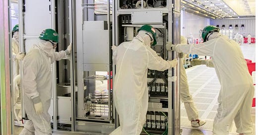
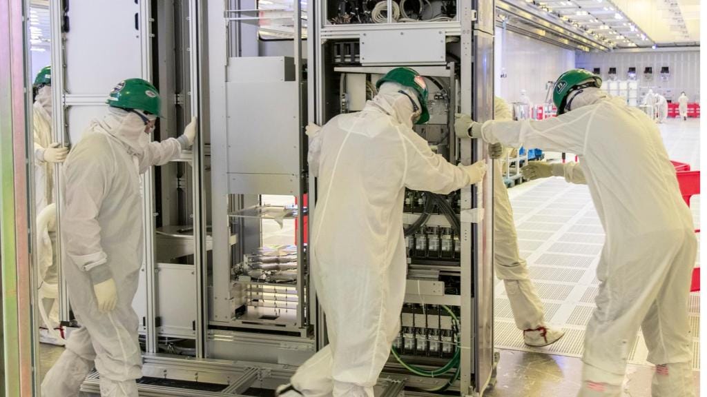
Intel recently put out a press release about Ireland’s Fab 34 in which they announced the first tool had been shipped in. The tool in question was called a lithography resist track for EUV by Intel. This tool coats a wafer with photoresist solution by spinning it rapidly. It then passes the wafer on to the lithography tool which reflects light off a mask, exposes the photoresist, and causes a chemical reaction which changes the solvency of the photoresist. The wafer then gets handed back to this tool which bakes the wafer, develops the photoresist, and then rinses away the residual photoresist. We describe the process in detail as well as technological developments and the competitive dynamics within the photoresist and track markets in this article.
The tool that Intel shipped didn’t come from the manufacturer though. It came from Intel’s Oregon facility. That’s very odd given the tool is a CLEAN TRACK LITHIUS Pro Z from Tokyo Electron.
Why is this so odd you may ask?
Because SemiAnalysis has independently confirmed that Intel is taking delivery of at least 2 more of these exact tools in the US before the Ireland tool is running EUV wafers.
This tool is the only kind in the world that can coat and develop a wafer with EUV photoresist. Tokyo Electron has 100% market share.
These tools are delivered by plane.
Why is Intel disassembling a tool in Oregon, shipping it to Ireland by plane, just to take delivery of the exact same tool by plane from Tokyo Electron?
Is Intel trying to abuse the upcoming CHIPS Act subsidies? Remember the CHIPS Act subsidies only apply if the tool is installed and used in the US.
So in that way, it makes complete logical sense to ship existing tools out of the US into other fabs, so new orders can take advantage of subsidies. This seems pretty freaking devious don’t ya think?
We asked Intel for a comment, and this is what they replied.
It is correct that we are shipping some prior-generation tools from Oregon to Ireland. These tools were previously used for technology development, which we do in Oregon. They are now being transitioned into high volume manufacturing in Ireland, while current generation tools are installed in Oregon for a new technology development cycle. This is a completely normal part of our process to extend the useful life of tools, and something we have done for many years. In fact, we also ship tools back to the US, and among our fabs worldwide.
We take issue with some of these statements. We went deep down this rabbit hole and asked our unofficial contacts for more info. We’ll share what we learned.
The tool in question being shipped into Oregon and shipped out of Oregon into Ireland are both CLEAN TRACK LITHIUS Pro Z from Tokyo Electron. There is no next generation of this tool released. With that said, the tool is not identical. Semiconductor capital equipment firms are constantly upgrading tools whether its software or new experimental features or process flows. In this case, the new tool Oregon is receiving has a new pre-exposure bake that has been added. This tool will be used to experiment with metal oxide photoresist in the future. Physically the new tool is still essentially identical though.
Intel has a philosophy and manufacturing principal called “Copy Exact”. In essence, Intel makes every environmental and process condition identical down to the generation of tool. This has been amazing for Intel because they can ramp nodes in new fabs very easily because they ensure all conditions are identical. Copy exact has also hurt Intel in the past in some cases because they continue ordering outdated tools and won’t switch to newer, more efficient generations.
A classic example of copy exact being damaging is with lithography tools from Nikon. Intel has purchased Nikon’s inferior lithography tools for some parts of their process flow despite objectively superior ones being available from ASML. They have remedied this, but it was a practice that existed for over a decade. Every other major fab such as TSMC and Samsung had long since reduced order volumes at Nikon heavily and moved volume over to ASML.
With copy exact, Intel is shipping an existing tool which is known to work well for the Intel 4 test chips. Intel is ensuring no variables changed, to gaurantee a good ramp of the node. At the same time, they are shipping a tool with a new experimental feature to Oregon, the main development and test fab, so that can develop them for future nodes.
Another underappreciated aspect of semiconductor manufacturing that an unnamed friend inside Intel described was the incredibly complicated multivariate calculus that involve tool positions, run times, throughputs, variance in time between tools, the wafer highway that transports wafers across the fab, and much more.
Think about it, a semiconductor fab is thousands of multi-million-dollar tools passing crystallized silicon back and forth to create billions of on-off switches that are perfectly interconnected to do calculations. There are hundreds of genius engineers whose job it is to solve the problem of optimal layouts of these fabs in order to maximize throughput per unit of cleanroom space and tool. Here is some b-roll from inside the fab to demonstrate our point.
The Oregon fab is being expanded and reconfigured constantly because it is the test development fab. There is some high-volume manufacturing there aswell. Intel likely cannot reconfigure the fab entirely the way they’d like without disassembling and moving some tools anyways. In this case, it makes sense to send some tools elsewhere while the fab is reconfigured and expanded.
On the topic of subsidies, Intel also responded with the following:
This has nothing to do with subsidies, and certainly nothing to do with subsidies under the CHIPS Act. The CHIPS Act is not yet funded by Congress and there is neither an application process nor a disbursement mechanism, which will take further time to set up once funding is allocated to the Commerce Department.
We don’t entirely agree with Intel’s comment on application process and disbursement mechanisms. While the funding isn’t set in stone, it’s pretty well defined in the House and Senate versions of the CHIPS Act. Remember, part of the CHIPS Act has already passed in past, but the money was never allocated. The commerce department is ready to start doling out cash for projects immediately when congress allocates the money. Intel and the government have had some pretty extensive interactions and even press conferences.
With that said, we agree the tool movement has nothing to do with the subsidies, but hopefully you found this rabbit hole interesting. Behind the subscriber only wall is some information about the photoresist, metal oxide resist, and the coater/developer market that is heating up with competition. Including a name I think is worth investing in for the long term.


