LAM Research (LRCX) Dry Deposit and Resist Could Become a Multi-Billion Dollar Business
LAM is a semiconductor processing and fabrication equipment designer and manufacturer who has announced a new dry photoresist technology in collaboration with IMEC and ASML. This new dry technology differs from the wet photoresist currently used in all commercial semiconductor foundries such as TSMC, Intel, Samsung, Micron, Global Foundries and SK Hynix.
Tokyo Electron stands to lose the most with the adoption of this new technology. TEL has leading market share in wet deposit and develop for photoresist. LAM is squarely targeting their incumbent position for future leading-edge nodes that utilize EUV. With current DUV nodes, the wavelength of light used during exposure is 193nm. EUV is an industry changing breakthrough which brings the wavelength down to 13nm. TEL will continue to supply wet deposit and develop for DUV nodes and most early EUV nodes, but without a large step forward in technology, they will lose the market which they currently dominate.
Taking a step back, wet photoresist is a photo-resistive chemical which is suspended in a solvent. This solvent is then deposited onto a wafer and spread by spinning the wafer rapidly. This solvent chemically reacts when exposed to high powered photons from the litho-exposure step. In the case of positive resist, the reacted solvent can be washed away after exposure, during the development step. This method is effective, reliable, and fast on DUV nodes.
Issues with wet photoresist begin to arise as Moore’s law trudges on and the lines being drawn are just tens of atoms across. The solvent which suspends the photo-resistive chemicals becomes problematic with these new nodes because the reaction becomes stochastic at the nano-scale. This contrasts with LAM’s new dry photoresist which reacts in a more predictable manner.
These stochastic defects lead to a variety of issues with the future 3nm/2nm nodes. One of these issues that can be mitigated by moving to dry deposit and develop is line collapse. When the solvent is washed away, the lines can become unstable and collapse. Other issues such as line edge roughness are also mitigated when moving to a dry deposit and develop flow.
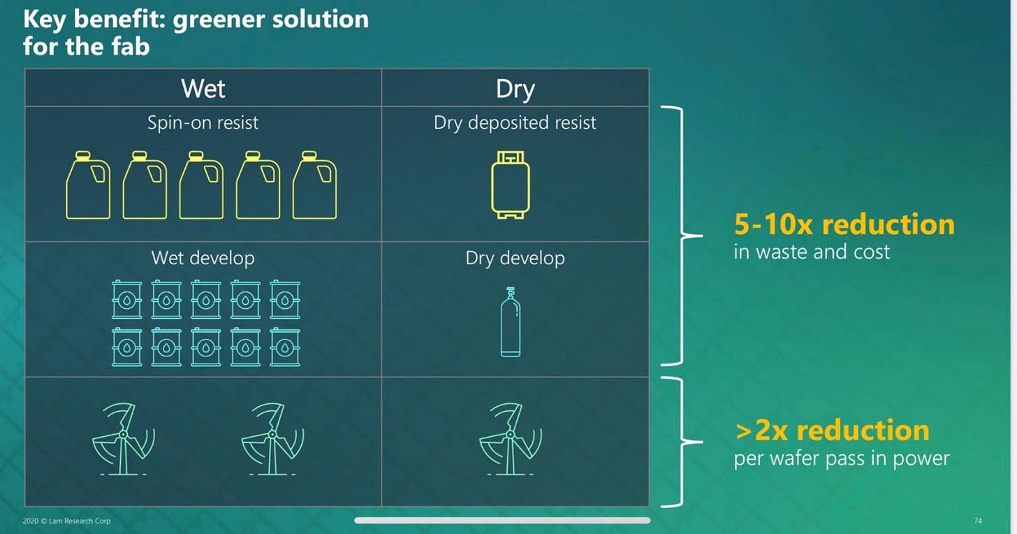
LAM’s dry photoresist also has advantages in areas outside of feature size fidelity. Namely, it requires significantly fewer chemicals and power. Pitching the green angle is relevant as semiconductor fabs run through tons of power and the chemical supply chain is quite destructive to the environment. Although the savings from power and chemicals are large, they are far outweighed by the much higher capital intensity of the new tools. Regardless, a greener fab is a noble goal and is critical for a sustainable future.
In the coming 5 years, Lam is targeting $1.5B of revenue for dry photoresist equipment. Beyond this, their revenue share in photoresist will continue to grow. Initially this will be driven by logic moving to ever smaller feature sizes to try to keep up with Moore’s Law. DRAM and emerging memories will begin to use this technology as well though. Despite DRAM area scaling moving at a glacial pace, the extreme sensitivity to cost could mean the jump into dry photoresist is a larger market than for logic. There are far more DRAM wafers processed on leading edge dram processes than there are for leading edge logic. The technology will need to be proven on logic nodes first of course.
There are parallels here to the EUV ramp, which is also being driven by logic. Samsung has begun using EUV sparingly but is still only on a minority of its total DRAM wafer output, but in a few years, EUV will begin to ramp hard to keep bending the cost curve lower. SK Hynix and Micron will follow suit in the coming years. All three will move to dry photoresist once the throughput is high enough and there are tangible cost savings.
The dry photoresist technology LAM has developed could become a multiple billion dollars business by the end of the decade. It will be a higher gross margin compared to the LAM corporate average of 46%. The financial impact of this new growth engine means a lot for investors. Investors should be very wary of TEL as this isn’t a growth area, there will be market share losses, and the bleeding could be ugly.
This article was originally published on SemiAnalysis on May 22nd 2020.
Clients and employees of SemiAnalysis may hold positions in companies referenced in this article.


