ASML published some very interesting data regarding wafer supply across various process technologies. Furthermore, they held some discussions about the long-term lithography intensity they expect. Lithography intensity is defined as the percentage of cost associated with lithography tools versus other wafer fabrication equipment tools. This report is a follow-up to last week’s piece on ASML.
First, ASML showed their estimates for millions of wafers per year. These are quite interesting to dive into.
The growth rates from 2015 to 2020, 2020 to 2025, and 2025 to 2030 are noteworthy.
Mature logic acceleration is the obvious oddball when comparing the last decade to this one. In advanced logic, the denominator is shifting from nothing to something much larger, so not that crazy. What we find very noteworthy is the DRAM figure. DRAM shrinks slowed down a lot in the early to the middle part of the last decade. ASML sees the wafer volumes growing rapidly in the 2025 to 2020 period, which is required if bit growth remains at 10% to 15% annually.
The oddest part is how much wafer growth for DRAM tails off in the 2nd half of the decade. This would make sense if there were a tremendous uplift in the number of bits per wafer, but ASML does not believe that will happen. We will get to that later.
NAND, on the other hand, despite having tremendous density increases, which are expected to continue into the latter part of the decade, continues to have colossal wafer volume growth as well. The big reason is that bit growth for NAND in the long term is expected to remain around 30%. 2023’s tepid growth is assumed to be an anomaly.
Inefficient wafers are a significant point of concern with ASML’s estimates.
ASML’s argument around more inefficient wafers due to technological sovereignty and foundry competition is reasonable, but only to some extent. They argue that 10% of total installed capacity worldwide will be inefficient by the decade’s end.
Compare that to 2015, when ASML believed there was no inefficient wafer capacity. The long-term utilization rate for fabs is around 80%, which is about what they were in 2015. If ASML is correct in that 10% of total installed capacity is inefficient by the decade’s end, does that bring utilization rates even lower to the 72.7% range?
Furthermore, when looking at incremental capacity, the picture looks even worse. 20% of the wafers added from 2025 to 2030 are considered inefficient by ASML.
How is none of the buy side or sell side screaming about this massive risk to their long-term guidance?
ASML’s wafer capacity model is questionable. The stool's other leg is the wafer mix's lithography intensity.
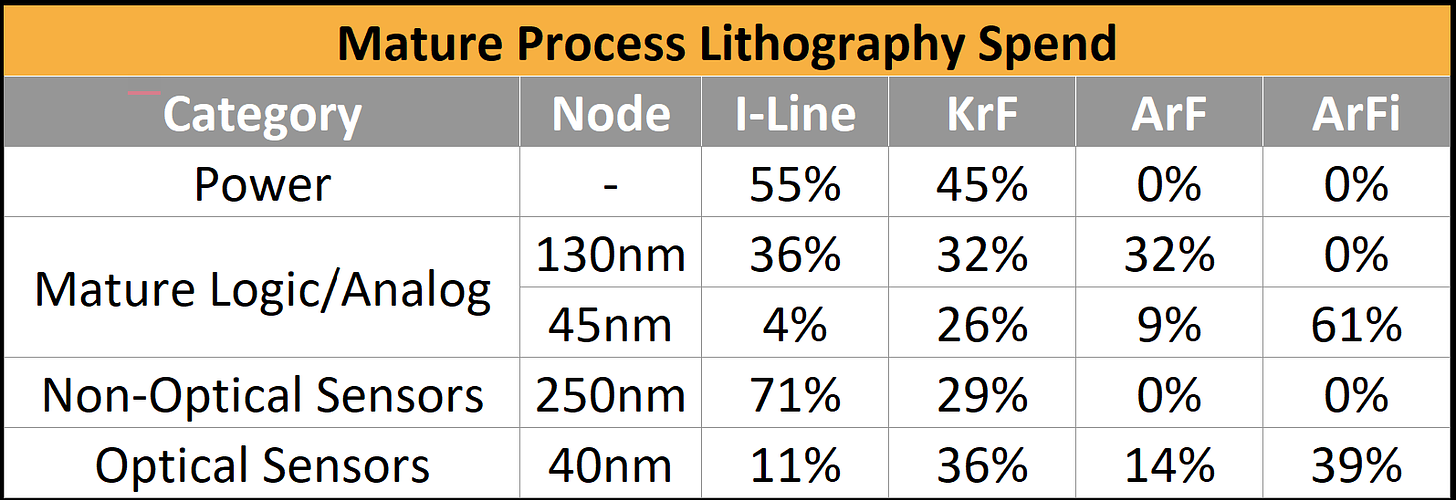
With mature process technologies, there is tremendous wafer growth, but some of it is in areas where Nikon, Canon, SMEE, EVG, and others are competing. SMEE, China’s lithography champion, is a dark horse that could take a significant share in I-Line and KrF. SMEE’s ArF and ArFi tools still do not work, but that could change over the next handful of years. Despite Nikon's rapid improvement in recent years, we still assume ASML controls most of the ArF and ArFi markets.
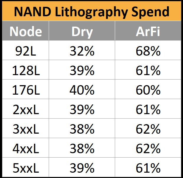
Most lithography demand will come from advanced logic, DRAM, and NAND. We will start with NAND first, as that is the process technology group with the lowest lithography intensity at 10% to 12%
The secular trend in NAND is that lithography spend will continue to scale slower than the rest of the process cost. ASML projects >10% growth in lithography cost per node. Outside of separating CMOS and cell wafers and increases in deck count, there doesn’t seem to be much driving lithography intensity up. In the latter half of the decade, lithography tools may fall under 10% of the total cost of a NAND fab from a WFE perspective.
Next, we will discuss DRAM and Logic; this includes a by-layer breakdown of lithography use on a high volume 5nm process technology. We disagree with some of ASML’s thoughts here, especially with regard to 3D DRAM and nanosheet lithography intensity.


