Meta Custom Silicon: What's Old Is New
Semi-Custom Silicon For AI and Video, Roadmap, Co-Design Partners
Meta just made a whole host of announcements related to their internal AI infrastructure and silicon. Some of the topics included moving to datacenters with more liquid cooling, higher power, and facility level changes. On the silicon side, funnily enough, Meta is taking the exact same strategy as Google.
Meta is only talking about the old chips they already have, just as the new stuff is nearly ready. For example, they released an entire blog on a research cluster they built last year with 16,000 Nvidia A100’s, only once they had already started building the much larger clusters with H100. That H100 cluster, as we reported in the past, has a very bizarre infrastructure setup.
This report will cover the old chips that Meta has had since 2021 as well as the new chips Meta has in development currently. We will discuss architecture, roadmap, various design partners, and future ambitions.
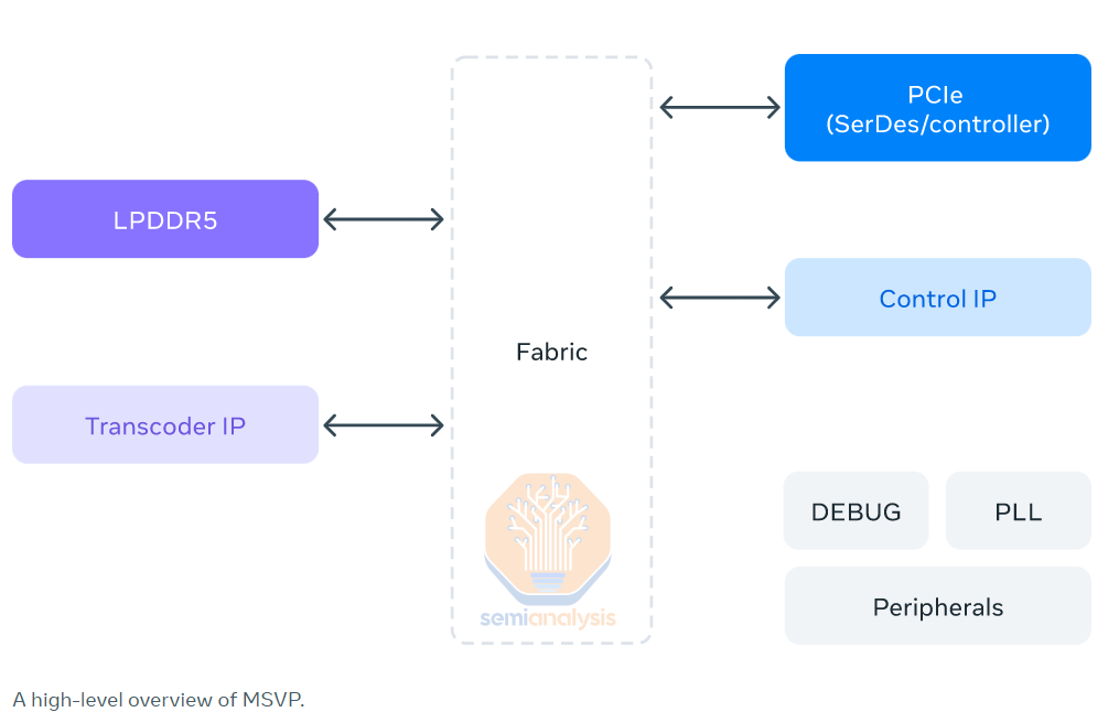
Meta Scalable Video Processor (MSVP)
Meta is showing off their video encoding ASIC which they have been deploying since 2021. The video encoding ASIC is an incredibly important piece of infrastructure for companies. For example, it is the primary reason Amazon has to offer significantly worse live streaming services with Twitch versus Google’s YouTube.
Google was the first to design a video encoding chip, codenamed Argos, which we covered years ago. The Google Argos VPUs deployed at scale do the work of over 10 million Intel CPUs for VP9 encoding, saving Google billions in cost. We have also covered NetInt’s VCU, a startup with a similar video encoding ASIC which is being sold to companies such as ByteDance, Baidu, Tencent, and Alibaba.
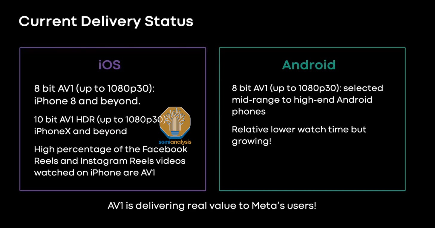
Meta has tremendous amounts of videos uploaded to Instagram and Facebook, so this product is critical to reducing costs. Furthermore, the 2nd generation of Meta’s Scalable Video Processor is what enables them to deploy AV1 in reels so pervasively. Note Meta only disclosed the 1st generation today.
Meta claims this chip was developed in-house, but that is not true. Both the announced MSVP and the upcoming next-generation version are co-designed with Broadcom. Google’s 1st two generations of their video encoding ASICs were also co-designed with Broadcom.
Each MSVP ASIC chip boasts a maximum transcoding capability of 4K, operating at 15fps under the highest quality setting with a configuration of one input stream to five output streams. It has the ability to scale up to 4K at 60fps under standard quality configuration. Meta claims the performance scales uniformly with the increase in resolution. All of this is accomplished with an approximate power usage of 10W for the PCIe module. There is a 9x performance boost for H.264 and 50x for VP9.
The chip comes in a M.2 22110 format supporting 4 lanes of PCIe Gen 4, so 8GB/s. There is also 2x 4GB of Micron LPDDR5 in the presented board, for a total of 8GB with 88GB/s of memory bandwidth. The package is about ~24mm by 19mm, and the die size is ~112mm^2.
The chips shown in Meta’s video were produced from June 21st to June 27th.
Meta Training and Inference Accelerator (MTIA)
AI is the most important and costly workload in Meta’s datacenters. Meta has been developing their AI chips since at least 2019. The first generation was just announced, and while the category of processor is named Meta Training and Inference Accelerator, to be clear, the first generation is only usable for inference.
Meta’s primary workload is DLRM inference today, and as such, they tried to architect their chip, especially for that workload. As a reminder, DLRM models are still the largest at-scale AI workload. These DLRMs are the backbone of companies like Baidu, Meta, ByteDance, Netflix, and Google. It is the engine of over a trillion dollars of annual revenue in advertising, search ranking, social media feed ordering, etc.
While generative AI will overtake it in hardware demand soon, that flip over hasn’t happened quite yet. Check out our prior dive into DLRMs here.
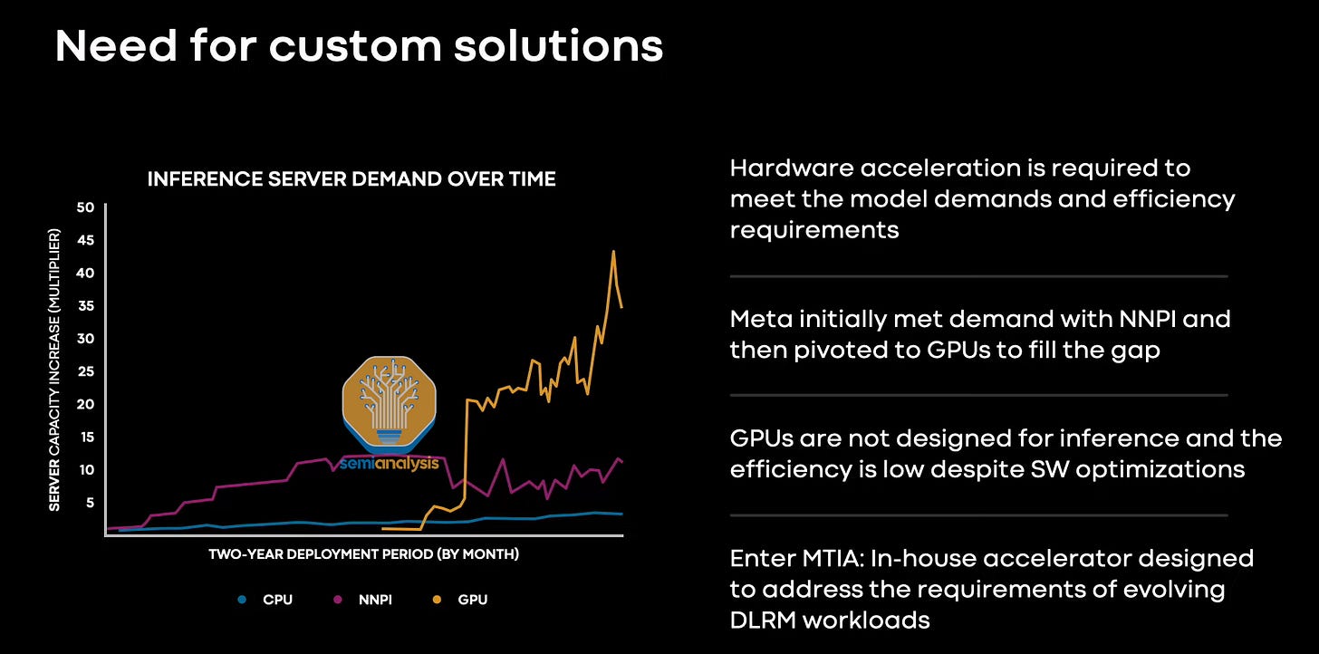
DLRM models are continuing to grow, and that is leading to significant infrastructure changes for Meta. For a period of time, they heavily utilized Intel’s NNP-I inference accelerator, but that quickly made way to GPUs. In some ways, the first-generation MTIA can be thought of as a second-generation NNP-I because the system architecture (not uarch) is very similar.
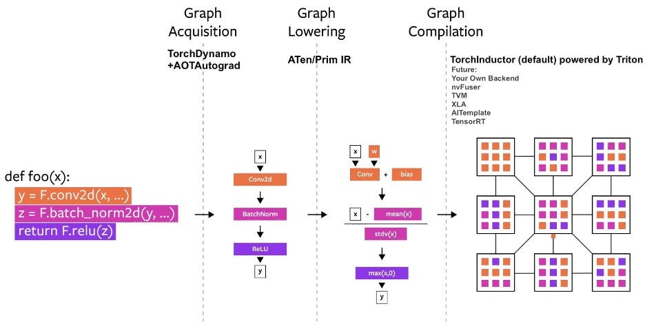
Meta launched their semi-custom AI accelerator program many years ago, and their goals were very clear. Lower cost inference for better DLRM models, and ease of use. Their first generation can be thought of as a software vehicle to develop the ability to utilize eager mode and full graph mode of PyTorch 2.0 with LLVM compilers. They are working on implementing Dynamo, Inductor, and Triton.
How Nvidia’s CUDA Monopoly In Machine Learning Is Breaking - OpenAI Triton And PyTorch 2.0
Over the last decade, the landscape of machine learning software development has undergone significant changes. Many frameworks have come and gone, but most have relied heavily on leveraging Nvidia's CUDA and performed best on Nvidia GPUs. However, with the arrival of PyTorch 2.0 and OpenAI's Triton, Nvidia's dominant position in this field, mainly due to its software moat, is being disrupted.
Our data shows Meta is the largest individual buyer of Nvidia’s H100 GPUs this year. That’s no coincidence. Meta needs GPUs for both training and inference and the H100’s is the most cost-effective way for them to serve this need in most cases.
Meta shared a profile of their various production recommendation models. These models have varying sizes and complexity. Meta also shared the performance of various hardware in these workloads.
While Meta did not share which GPU they were comparing to, we asked around, and it seems to be old Ampere GPUs, not new Hopper and Lovelace GPUs. While this seems unfair, remember Meta’s 1st generation MTIA is also an older chip. Once you stack on the additional performance of the new Nvidia chips, the first-generation MTIA loses in most workloads on performance per watt.
With that said, the first gen MTIA is just a start. Let’s dive into the chip before discussing the next generation, roadmap, and design partners.
Meta got the chips in the video back in 2021. The MTIA is fabricated on TSMC’s 7nm fabs and packaged by Amkor. The chip markings state this occurred from August 23rd to August 29th of 2021.


The chip has 102.4 TOPS of INT8 and 51.2 TFLOPS of FP16 with a 25W TDP. There is a total of 128 MB SRAM which runs at 800GB/s. This SRAM sits next to the memory controllers and can act as a memory side cache of directly addressed as addressable memory. There is also up to 128GB of LPDDR5-5500 on a 256-bit bus running at 176GB/s. It’s noteworthy that Meta used LPDDR5 which is capable of 6400 MTs, but run it downclocked. There are also 8 PCIe 4.0 lanes.


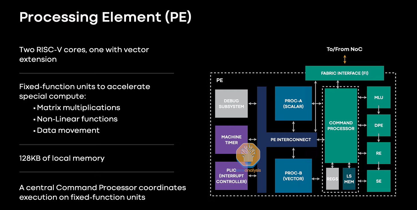
The memory and IO sits around the processing elements. These processing elements are an 8 by 8 grid containing a command processor, local memory, and two different RISC-V CPUs from Andes. One core has only scalar capabilities, and the other can do both scalar and vector. These cores are licensed from a third-party IP house. That third party does not assist with the backend.
There are also a variety of fixed accelerators to accelerate matrix multiplications, non-linear functions, and data movement.
Physically the chip sits on a PCIe Gen 4x8 dual m.2 card in Delta Lake servers connected to Intel Copper Lake CPUs with 96GB of DDR4 and PCIe 3.0 x24 connection to nested switches (80 lane Broadcom PCIe4 switch).
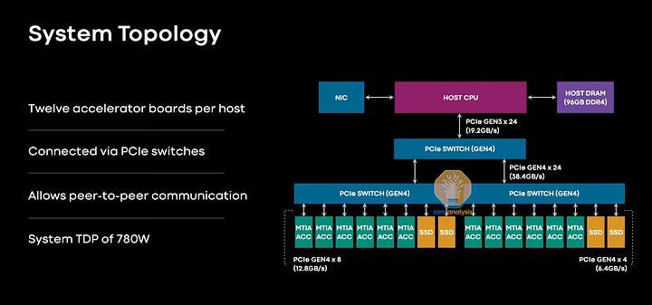


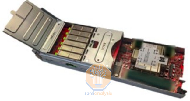
There are 12x MTIA per host, and the entire system consumes 780W.
Silicon Co-Design Partners and Roadmap
Next, we will discuss the roadmap, chip codenames, the future of MTIA, and where it is useful vs not.


