NAND Flash Monopoly Broken? Tokyo Electron Moly Dep + Cryo Etch Takes On Lam Research For The Future Of NAND
>$1B Billion Dollar Revenue Impact Lam Research ‘25 Revenue from Cryo Etch + Moly Dep?
Moore’s Law for digital logic and DRAM has all but died with the density and cost improvements advancing at a glacial pace. This is not the case with NAND Flash memory. Unlike the rest of the semiconductor industry, NAND has enjoyed massive yearly cost decreases.
This is because NAND flipped the formula and stopped relying on lithography for patterning smaller cells. Instead, NAND has relied on a different architecture, 3D NAND, first commercialized in 2013. Since then, NAND makers have improved NAND’s density and cost structure by adding more and more layers of memory cells. The focus shifted almost entirely from lithography to deposition and etch processing steps. As a result, since 3D NAND was introduced, density has improved by 30% per year at a very consistent rate.
Today we will be covering the NAND semiconductor market, process technology scaling avenues, manufacturing process, NAND pricing trends, the current glut/future shortages, 2023 to 2025 NAND wafer fabrication equipment spend outlook, Western Digital and Kioxia’s future, YMTC, a potential sanction violation, a deep dive into the high aspect ratio etch market for NAND, 3D DRAM possibilities, the big upcoming material change in deposition, and a potential big shift in market share from Lam Research to Tokyo Electron (TEL) due to two manufacturing changes representing over $1 billion of revenues potentially changing hands.
As always, the technology background will be detailed for everyone. The 2 new developments in deposition and etch for NAND, 3D DRAM possibilities, business impacts, changes, high-level takeaways, and WDC/Kioxia commentary will be detailed for subscribers. We include market intelligence gathered on the ground from tool firms and NAND manufacturers from VLSI Japan and Semicon West.
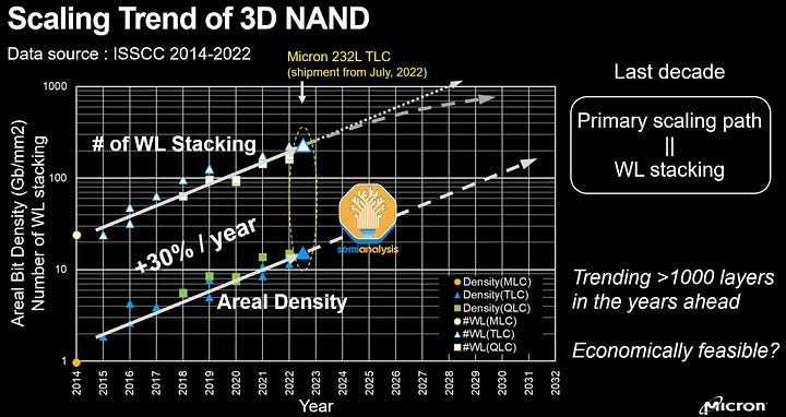
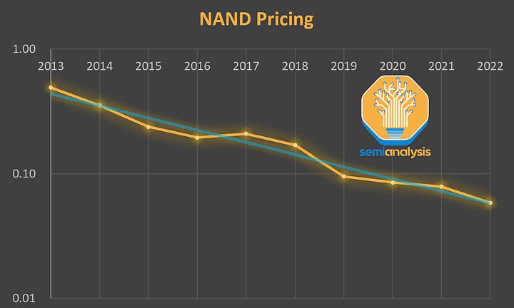
This increase in density has allowed NAND cost per bit to decrease around 21% annually since the introduction of 3D NAND, and scaling is expected to continue although there may be some challenges ahead. Micron believes that NAND cost per bit can continue to decrease at a low to mid-teens percent annually, whereas DRAM is harder to scale, only targeting high single-digit percent annual cost reductions. This low to mid-teens is a regression from the 21% that the industry has experienced up until recently.

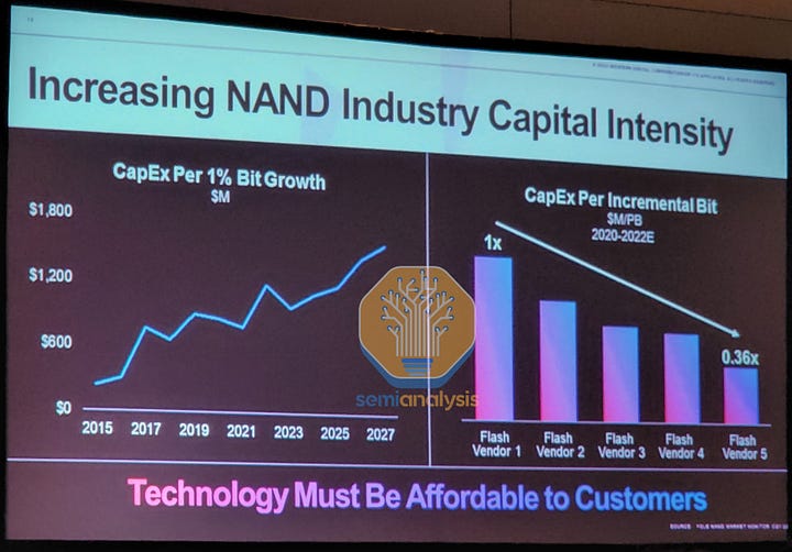
The end result is that despite the total equipment purchases for NAND fabs being ~$15 billion every year from 2018 to 2022, the total capacity for NAND has consistently grown by more than 30% annually. This is primarily due to manufacturing efficiency improvements. However, continuing to grow capacity will require a proportionally larger Capex going forward (Capex intensity) unless new equipment innovations are brought to market. On the other hand, there is currently a massive glut of NAND in the market due to the current semiconductor downturn, so large Capex projects are being delayed. This is leading to the perfect setup for a shortage in 1.5 years.
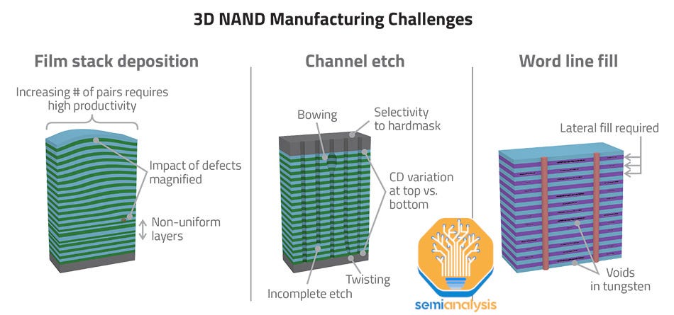
The primary reason for these massive cost improvements in NAND is that fabs could increase density without massive commensurate increases in process step counts. The most critical steps in 3D NAND are the thin film depositions, and high aspect ratio etches.
An oversimplified manufacturing process for NAND is that alternating films are deposited, then there are a few different etches that go through the stack and split the cells/connect them up to the outside world. Lam Research is the leader in many of these process steps, including, most critically, the high aspect ratio etches.
The 4 Avenues of NAND Scaling
There are 4 main avenues for scaling the storage capacity of NAND Flash per wafer.
Logical scaling – The number of bits stored per cell. This requires storing 2^n voltage levels per cell.
Vertical scaling – The number of NAND cells stacked vertically
Lateral scaling – The size/number of cells that can be fit on the 2D vector
Architecture scaling – Various techniques to increase density and reduce overhead from cells/periphery.
One method is Logical Scaling, by storing more bits per physical memory cell. Each additional bit stored per cell requires doubling the number of discernible voltage states the cell must hold. IE: 2 voltage levels for 1-bit per cell (SLC), 4 voltage levels for 2-bits per cell (MLC), 8 voltage levels for 3-bits per cell (TLC), 16 voltage levels for 4-bits per cell (QLC), 32 voltage levels for 5-bits per cell (PLC).
Ideally, this gives ‘free’ scaling by increasing stored bits without increasing the physical number of memory cells. 4-bits per cell, QLC, arrived in 2018, and the Solidigm team that SK Hynix acquired from Intel has been talking up 5-bits per cell, PLC, Floating Gate NAND. Researchers at Kioxia even demonstrated 7-bits per cell in cryogenic conditions back in 2021.
However, the major downside of logical scaling is reducing the number of electrons per stored State. Increasing the number of voltage states per cell means dividing the electron-storing capacity of each memory cell. Fewer electrons per state increase variability and destroys reliability. 2D NAND has already hit the limits of this with TLC technology, with 3D NAND fast approaching similar limits. Going forward, we are starting to see the effects of this that signal the end of logical scaling.
Manufacturers are finding that making even smaller cells (lateral+vertical) that each holds fewer electrons makes higher bits per cell untenable. For example, Solidigm’s 192-layer PLC failed and will not ramp to large volumes due to an inferior cost structure.
Samsung’s >236-layer V9 generation of 3D NAND also shows poorer generational scaling for QLC vs TLC. In the V7 generation, QLC is 40% denser than TLC. With V9, QLC is only 20% denser than QLC. This is because the QLC memory cell cannot shrink as much as the TLC cell. As such, Micron and SK Hynix believe TLC (3 bits per cell) NAND will be the most cost-effective long-term solution.
Next is Vertical Scaling, the primary avenue for density gains over the last decade. The current high aspect ratio (HAR) etch depth limit is 6 to 7 microns with the minimum thickness of each cell being about 40nm. So far, manufacturers have only been able to achieve up to 128 Word Line layer stacks (~50nm each). Going beyond this requires string stacking of multiple decks etched separately and combined atop the other. Solidigm’s 192-layer design uses four 48-layer decks, while the latest 238-layer generation from Hynix uses two decks with 119 active Word Lines each.
Ideally, the fewer decks, the better, as fewer manufacturing steps need to be repeated, with a lower risk of alignment errors when stacking decks. Otherwise, the only other ways of vertical scaling is to reduce the Z thickness of each memory cell and Word Line, or to increase the HAR etch depth which we will detail below. This is why Tokyo Electron could take lots of business from Lam Research. The deposition change we describe later could be just as impactful.
Then we have the traditional Lateral Scaling in the X and Y direction. This can be done by increasing the density of memory channel holes or by reducing the area overhead of the slits and memory block subdivisions. The former is already tapped out as the holes can’t get much smaller with the need to fit all the layers on the sidewalls to form the charge trap cell. The spacing between holes is also currently as tight as possible.
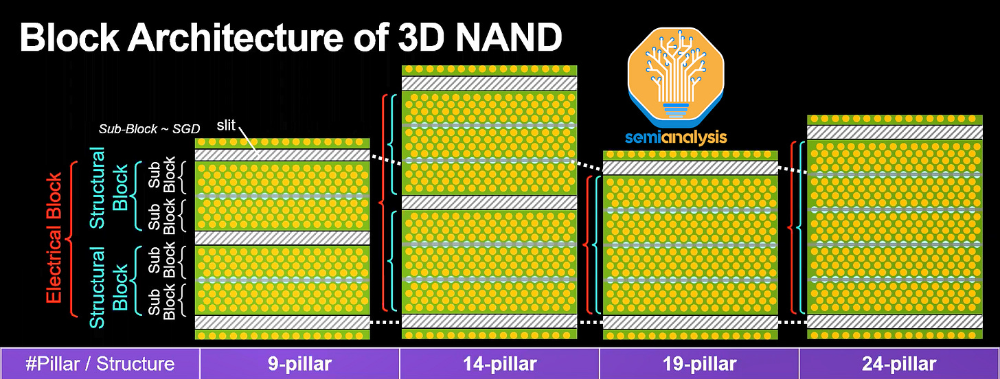
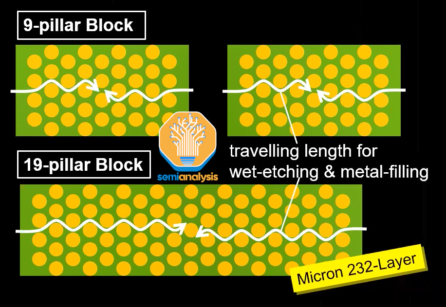
For the latter, Micron and WDC/Kioxia are increasing the number of channel holes between slits, reducing the total number of slits and thus achieving better area utilization with holes. This means that their replacement gate process has to travel deeper into the layers horizontally to remove all SiN residue properly and do the subsequent W fill cleanly.
The industry standard since the 64-layer generation has been 9 pillars between slits. Micron 232-layer has gone to 19 pillars between slits, while WDC/Kioxia BiCS6 162-layer goes to 24 pillars between slits, although we haven’t found this broadly ramped in the market. Their 218-layer BiCS8 takes things one step further by removing the need for a dummy row of holes to separate the subblocks.
While the density gain from these lateral scaling techniques is minor compared to vertical scaling, it does enable a linear cost reduction without increasing WFE intensity. Aside from this, lateral scaling can also be done by reducing the area overhead from the staircases at the sides of the array by using a staggered staircase design. However, this comes at the cost of increased routing density and complexity of the hookup area to the Word Lines.
Lastly, we have Architectural Scaling, which focuses on where the CMOS logic peripheral circuits are placed. Designs went from a simple CMOS Next to Array, then more recently to CMOS Under Array, saving die area by building the circuitry below the NAND stack. However, there are limits to the CMOS logic process technology due to the harsh nature of the NAND array processing steps. CMOS Bonded Array (CBA) addresses this by fabricating the logic on a separate wafer which is then bonded to the memory array wafer with hybrid bonding.
This enables more advanced logic and higher routing density to achieve further lateral scaling of the staircase and sub-block divisions. The cost increase from bonding multiple wafers can be offset by reducing design/process complexity and cycle time as logic and memory are fabricated in parallel. YMTC led the way with its 64-layer Xtacking 1.0 and its amazing 1.0-micron pitch Hybrid Bonding. WDC/Kioxia BiCS8 218-layer will also adopt a Hybrid Bonding process, with other manufacturers following suit.
Most of these avenues of scaling are pretty much already tapped out. Vertical scaling has been the primary way to scale, but even that has also begun to tap out with current manufacturing equipment.
3D NAND Structure and Manufacturing Flow
Alternating layers of Oxide and Nitride films are first deposited onto the base wafer. Each layer is between 20 to 30 nm in thickness. The theoretical limit per stack can be over 250 layers high and nearly 7 microns tall. A thick hard mask is then added to prepare for the High Aspect Ratio (HAR) channel hole etch. This Reactive Ion Etch process digs an array of holes 70 times deeper than wide. Channel hole uniformity in roundness and across the entire depth of the hole is crucial in reducing memory cell performance variability. These steps are repeated for designs with multiple decks that are then stacked on top of each other.
From this, the channel holes are filled with multiple layers to form the charge trap cell, with each layer deposited on the sidewalls making the hole progressively narrower. Next comes the metal replacement gate process. Slits are etched down though all layers to form trenches that expose the sides of the stack. This allows access for the exhumation of the Nitride layers and subsequent deposition of barriers done through ALD and the Tungsten Word Line fill. Staircases are etched on the sides of the array to expose the Word Line layers to vertical contacts.
Finally, the Bit line and metal interconnect is formed above and connects with the fabricated CMOS circuits, which include Word Line drivers and other peripheral circuitry for the NAND interface. From this, we see that 3D NAND is highly dependent of HAR etch and deposition capabilities to scale density and performance.
As stated earlier, the primary limitation is etching the channel holes in the fabrication process. This is why raw process time per GB (and therefore process cost) scaling is expected to slow down from the historical trend we’ve observed. This is the focus of the piece.
NAND Market Update, Investor's Mirage: Is the Oasis Closer Than It Appears?
NAND continues to be weak, with massive overcapacity. Due to oversupply, utilization rates for the industry wafer starts are currently in the 60% range. The inventory situation is also huge. This is the worst supply and demand mismatch we have seen since 1997.
Now, the major NAND players are all lowering utilization rates in an attempt to reduce inventories and return the market to balance. However, there are still some investments required to make technology transitions. Samsung, the biggest NAND producer (34% of the market) is behind on its NAND process. Its current generation is still mostly 128-layer, and 176-layer NAND still only represents a small portion of the volume.
This is well behind SK Hynix and Micron, who are at over >200-layer technology nodes. Samsung is attempting to spend to transition the majority of their capacity this year to 236-layer. They are effectively skipping a node for a large portion of their production. While their investment in tech transitions will bolster NAND WFE this year, it will only delay the recovery as there is even more slack in capacity to absorb strengthening demand. Once the tech transition is complete, they will have brought another 70% more bits to market. Samsung wants to force consolidation, this is a tactic driven down from the very top of the firm.
China is also not there to save the day. China’s main NAND player, YMTC has been cut off from buying equipment. This ban makes sense because NAND is where Chinese players succeeded most in their internal chip efforts. It is unarguable that YMTC was a technology leader before the ban. They were pouring in capex to the market even during the downturns to keep scaling up their production and capability. The expectation was that this would have provided a buffer to supply during downturns. China being subject to export controls means they cannot support WFE spend anymore during downturns.
We believe 2024 will be an even leaner year for NAND capex compared to 2023. We only expect a strong recovery by 2025 when NAND supply and demand return to balance due to tremendous inventory and low utilization rates providing a buffer. Long term bit demand will continue to grow, and the industry needs investment to fulfill that demand eventually. Note this is very pitiful growth in the market. It also assumes some NAND consolidation which we will discuss below.
Below we will share our 2023 to 2025 NAND wafer fabrication equipment spend, Western Digital and Kioxia’s future, a deep dive into the high aspect ratio etch market for NAND, 3D DRAM possibilities, the big upcoming material change in deposition, and the potential big shift in market share from Lam Research to Tokyo Electron that could represent over $1 billion of revenues changing hands.


