Silicon Carbide Game-Changer: Aehr's Edge - SiC Pure Play $AEHR
From Electric Vehicles to Renewable Energy: Aehr Test Systems Tools Are Critical To Tomorrow's Future
Semiconductor manufacturing is the alchemical process of the modern era, a complex dance that requires the harmonious synchronization of thousands of companies and tens of thousands of process steps. Due to its complexity, yield is a more than $100 billion problem for the industry. As such, the fabrication process contains a constant stream of critical status checks to support the most complex thing humans have created.
A casual observer of the semiconductor industry will often over-focus on ASML and lithography, despite that only comprising ~22% of a semiconductor fab’s total equipment (in $ value). Metrology and inspection (checking) are ~13% of the tools (in $ value). Firms like KLA-Tencor KLAC 0.00%↑, Nova Measuring NVMI 0.00%↑, and Onto Innovation ONTO 0.00%↑ manufacture equipment that measures the wafer throughout the front-end.
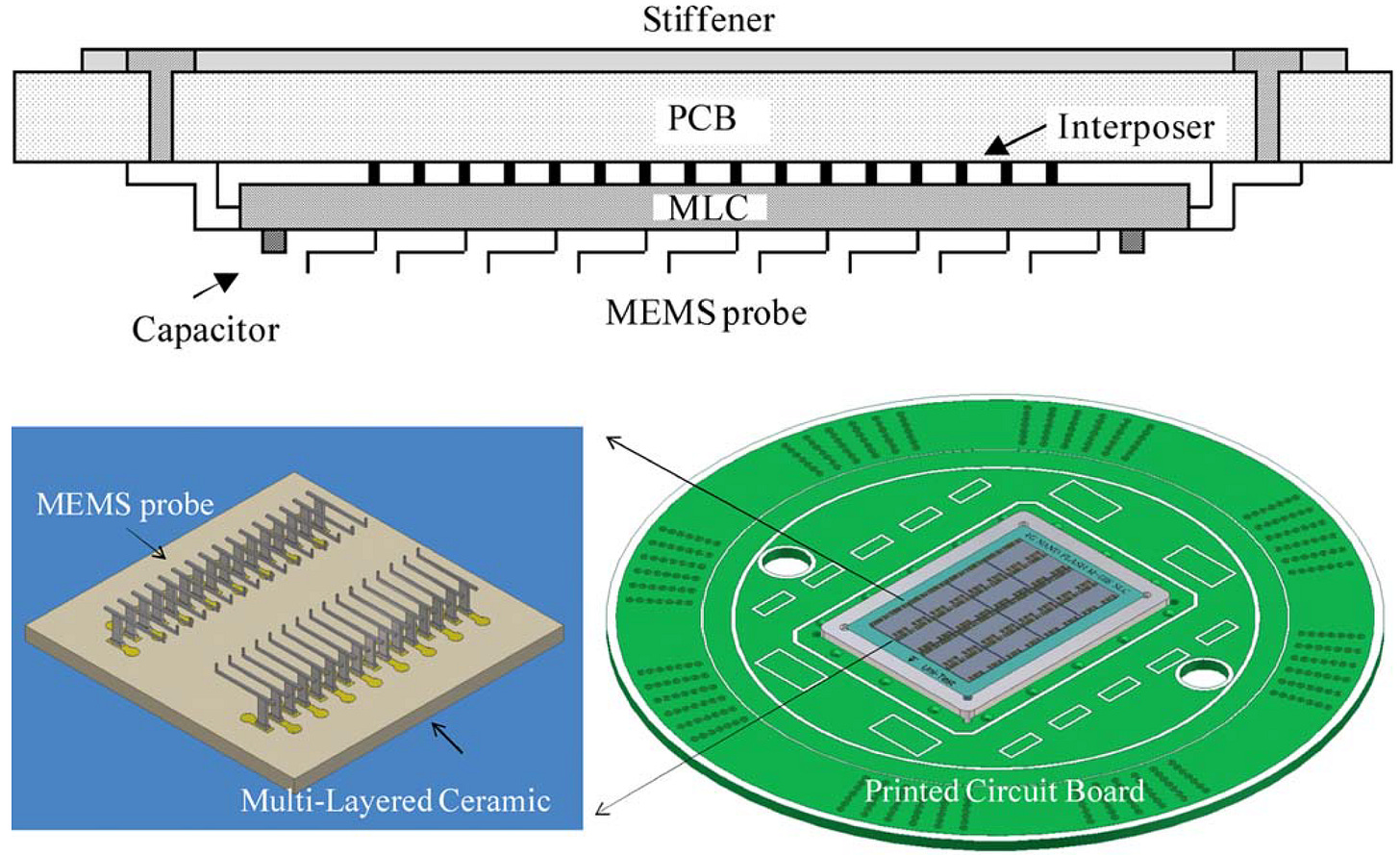
FormFactor FORM 0.00%↑, Micronics Japan 6871.JP, and Technoprobe TPRO.IT make probe cards that consist of a printed circuit board with an array of probes finer than a human hair. The arrangement of the probes is customized to every individual chip design. The probes themselves are so fine that they can only be manufactured on a MEMS wafer.
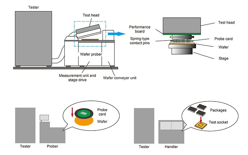
Advantest 6857.JP and Teradyne TER 0.00%↑ are most well-known for automated test equipment (ATE). Among many other things, ATE tools take the probe cards, line them up perfectly with the chips on the wafer, and make physical contact with the circuitry on the wafer. Then it sends precise electrical test signals to the circuits to characterize them.
That’s just a quick, incomplete summary of a few major firms, but there are many other firms in the “checking” industry. Today we want to discuss Aehr Test Solutions $AEHR, a small firm with a unique testing solution. It is used for Apple’s FaceID, Intel silicon photonics, and, most importantly, silicon carbide. We first published a report on the firm a couple of years calling out its early success in SiC. Since then, revenue and the stock price have soared due to the rapid adoption of their tools in silicon carbide. We have also participated in most earnings calls as analysts and visited their primary manufacturing facility.
Today’s report will dive into their unique test technology. We will explore the durability of Aehr’s competitive advantage versus multiple competitors and what those competitors are doing to reduce their technology gap with Aehr Test Systems. We will also include a model that considers EV requirements, tool throughput, consumables revenue ramp, test intensity, and more, indicating that Aehr’s opportunity is potentially more than $500 million annually. We will also discuss their potential for growth in GaN, silicon photonics, and memory devices. Lastly, we will discuss why Aehr is a better vehicle for long-term SiC and GaN growth versus Axcelis ACLS 0.00%↑ and Aixtron AIXA.
Due to its increased energy efficiency, Silicon carbide (SiC) is rapidly becoming the standard for high-power electronic devices. To support the explosion in electric vehicles, renewable energy, and energy storage, the industry is looking to increase wafer volume from a couple hundred thousand wafers a year to multiple million wafers a year by the decade’s end.
Failures in the electrification end markets are especially catastrophic because the automobiles and infrastructure are part of an installed base that should last decades. Furthermore, servicing and repair require taking apart a complex device in the field. These devices may function perfectly fine at normal temperatures when they are first fabricated, but failures and irregularities can become frequent over time when exposed to more extreme environments for an extended period.
Automotive and industrial suppliers require intensive testing to become a qualified supplier, and even once qualified, there’s no skimping out on testing. SiC has many defects related to its fragile/brittle crystalline structure. Major sources include substrate, epi, or doping-related defects such as threading dislocations, ingrown stacking faults, and recombination-induced stacking faults (RISFs). Yield here is especially low relative to other semiconductors and contributes to about 30% of the final device cost. In-field defect rates take this figure much higher.
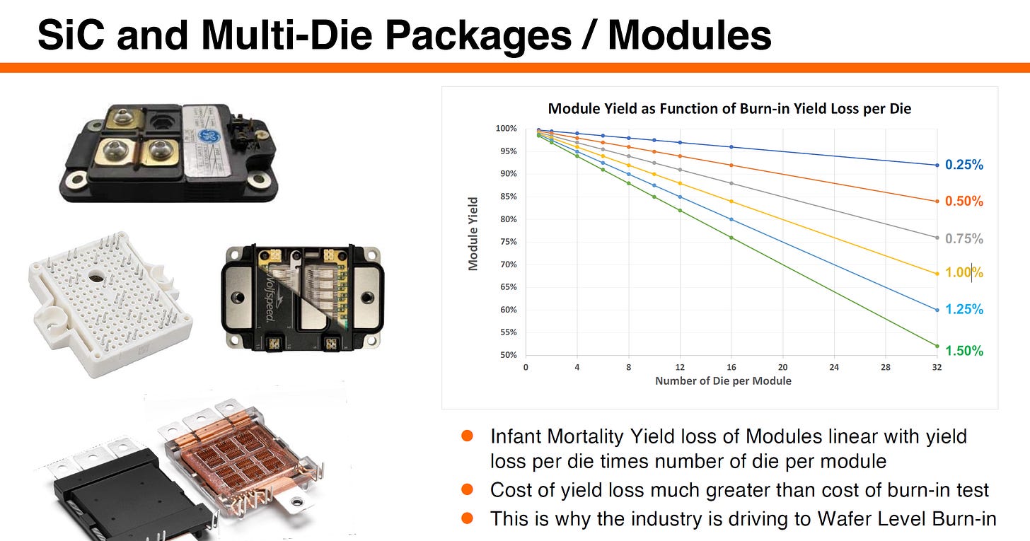
Testing in automotive can last two to four days per device, and the footprint required for testing thousands of devices is astronomical. Furthermore, most industry has moved from discrete power devices to multi-die modules. In these cases, even one bad die could cause many good dies to fail. With a decade-long failure rate of even 1%, the standard 12-die module will have a failure rate of ~15%!
The bathtub curve applies to semiconductors. Mortality rates are very high at the beginning of a device’s life cycle. This is called infant mortality. These high mortality rates exponentially decrease to a steady state. After a long period of low failure rates, failures eventually rise again due to wear-out failures. Infant mortality must be weeded out, but there are multiple ways to do so.
Most of the industry uses package or module burn-in to weed out infant mortality in high-value parts. Accelerated stress testing at elevated temp/voltages helps weed out rotting eggs by measuring any changes in the device’s performance during testing. These latent manufacturing defects can be pulled, minimizing the chances that a customer has a product die in the field. This is fine for the realm of IGBT and standard silicon-based devices because burn-in times are shorter, but with SiC, the costs begin to soar due to the length of burn-in time required. This is where Aehr Test System’s novel approach comes in. Instead of creating tools for testing on the module level, they make tools that test at the wafer-level.
The broader logic industry adopted an early version of these tools in the 90s, but then that transitioned away to more industry-standard testing. Aehr is still used for wafer-level burn-in for lasers, such as with Apple’s FaceID and Intel’s silicon photonics platform.
Due to poor yields with silicon carbide, a large portion of infant mortality can be weeded out. Allows fewer failed devices to be packaged and the full test cycle to be shortened. Cycle times are a major limiting factor in SiC device production, and Aehr's solution to decrease the cycle times is promising. On Semiconductor $ON is the first hallmark customer for Aehr in SiC. Aehr is also engaged with others such as Infineon, ST Microelectronics, Rohm, Wolfspeed, Mitsubishi, Rohm, Sanan IC, CR Micro, and more which we will discuss specific customer progress later.
The cost savings when moving to wafer-level burn-in are tremendous. If the automotive quality requirements hold, it is a no-brainer for every SiC device fabricator to move to wafer-level burn-in. As automakers become aware of it, some even require their vendors to implement very long burn-in of a dozen hours. As such, the only cost-effective way to do this is with Aehr.
Aehr has developed the FOX-XP tool for these wafer-level burn-in tests. Each wafer can contain as many as a thousand SiC devices. FOX-XP can test 9 to 18 wafers at a time. FOX-XP does this inside the chamber, which acts as a highly regulated extreme temperature environment. This can be considered an oven, except it, can dissipate over 18 kW too. The FOX-XP tools cost about $2.5M.
These tools must also be used with Aehr Test System’s WaferPak contactor. The WaferPak is similar to a probe card, but instead of only interfacing with the wafer, it also carries it. WaferPaks are considered a consumable as they are unique to each design and cost around $1.5M to fill out a FOX-XP. Designs typically change every few years. These design changes increase efficiency and reduce costs for end-market power devices.


WaferPaks are a critical engine for future reoccurring revenue. Our model, which we will share later, indicates that WaferPaks will exceed FOX-XP revenue within a handful of years.
The WaferPak has 2048 I/O pins and DPS channels. Each channel has remote voltage and ground sense. Each channel can cycle between 1024 voltage levels up to 40V and as low as -30V. It can run as high as 2A. To be clear, WaferPaks aren’t capable of as fine-grained testing as a high-end probe card because they have significantly fewer probes. Furthermore, these probes have far finer control than high-end ATE equipment. The critical point is that it allows for high-voltage testing while operating at temperatures as high as 150 degrees Celsius.
The burn-in tools are capable of multiple types of tests. This includes bipolar voltage with negative high-temperature gate bias, which was requested and developed rapidly for one of the new customers.
The last piece is Aehr’s product line, the FOX-XP WaferPak Aligner, which vacuum suction loads and unloads wafers between FOUPs or wafer cassettes and the WaferPak Contactors. WaferPak Aligners generally cost less than $1M, but there are various offerings depending on the fab's automation requirements. Aligners can support multiple Fox-XP tools, but many fabs will want to completely automate Fox-XP, which requires pairing them 1 to 1 with fully automated aligners.
Next, we will discuss Aehr’s specific wins with Onsemi and the status of orders/sales with Infineon, ST Microelectronics, Rohm, Wolfspeed, Mitsubishi, Rohm, Sanan IC, and CR Micro. Furthermore, we will share our detailed model that shows industry-level demand for wafers with electrification and burn-in tool requirements. This model also separately models WaferPak and Aligner sales. Consumables are an essential part of Aehr’s story.
We will also discuss competition and their penetration into this space, including Pentamaster, EDA Industries, and Teradyne. We will also discuss their potential for growth in GaN, silicon photonics, and memory devices. Lastly, we will discuss why Aehr is a better vehicle for long-term SiC and GaN growth versus Axcelis $ACLS and Aixtron AIXA.
All of this is in the second half of the report below, for subscribers.


