Sound The Siryn: AmpereOne 192-Core CPU
Chiplets, Advanced Packaging, and Disingenuous Performance Claims
Ampere Computing specializes in CPUs for the cloud datacenter market. The company had succeeded in attracting significant customer traction, with several major cloud providers, including Alibaba, Google, Microsoft, Tencent, and Oracle all buying varying amounts of Ampere's chips for their cloud operations. Furthermore, the Ampere chips can be found in Cruise self-driving cars as well. In 2022 alone, SemiAnalysis estimates Ampere shipped over 300,000 CPUs.
Today, Ampere Computing is announcing its 3rd generation datacenter CPU, AmpereOne codenamed Siryn. This marks a big change for the firm as it is their first with a custom in-house architecture. Ampere Computing previously used Arm's Neoverse core, but they have now successfully shed the shackles of Arm's costly and restrictive core licensing terms and embraced an Arm architecture license which offers greater freedom.
Today we will be diving into the performance, competitive positioning, strategy, and financial details of Ampere Computing’s new CPU as well as their upcoming IPO. We don’t agree with everything the company is telling people and think some of their comparisons are frankly disingenuous. Before we dive into critically analyzing what they have announced, let’s do a quick overview of the firm.
Cloud Native – Is it Marketing Fluff?
The main strategy of Ampere Computing is that they design and deliver CPUs purpose-built for cloud datacenters. This overarching strategy boils down to 2 words, “Cloud Native.” AMD and Intel must target their CPUs for a wide range of workloads ranging from various flavors of enterprise and cloud—these range from storage servers to web servers to accelerator-based AI systems. The CPU core designs for these applications from AMD and Intel CPU cores also tend to go into client computing applications like laptops with only a few modifications. Ampere’s claim is that they can laser focus on the fastest growing segment of the datacenter, cloud, and optimize their product for it.
They believe the future of computing will rely heavily on microservices, containerization, and serverless execution models. These concepts are generally about scaling performance out via a large amount small jobs and processes and not overly focusing on single-threaded CPU performance. Both AMD and Intel are releasing CPUs with similar strategies over the next year. Ampere believes there are 3 primary ways their CPUs are “cloud native.”
Higher performance per CPU
Predictable performance
Scalability
Let’s break down how their architecture achieves this. Ampere believes they can have higher performance by having higher core counts. These higher core counts can only be achieved by making a conscious engineering tradeoff to utilize smaller cores versus Intel and AMD. To be clear, Ampere cores are significantly behind AMD and Intel in the area of performance per thread, especially floating-point performance. Their bet is that these smaller cores offer higher performance per transistor and watt, which, when looking holistically across the whole chip, enables them to offer higher overall performance. We will discuss how this pans out in the performance section of the report.
Ampere also believes they offer more predictable performance by running only 1 thread per core. Intel and AMD offer 2 threads per core, simultaneous multithreading (SMT). SMT takes advantage of gaps in workloads primarily caused by waiting for memory and allows the execution resources of the hardware to be utilized at a higher rate. SMT increases performance while barely increasing the total silicon area and transistor count per core.
The downside of SMT is that it can cause unpredictable performance as threads share the core’s resources. Another potential downside is security. Exploiting vulnerabilities in SMT is a common method of side-channel attacks that have exploded in popularity since the advent of Spectre and Meltdown.
Ampere’s pitch of more predictable performance also extends to Ampere’s cache architecture. Each core has a large private L2 cache, while the shared L3 cache is relatively tiny. AMD and Intel generally rely on larger shared L3 caches which helps performance in many workloads but can also hamper the predictability of performance.
Ampere also places a large emphasis on clock speed consistency. Intel and AMD CPUs vary their core clock speed significantly based on how many cores or threads are in use and what type of code is being executed. This helps their CPUs maximize performance within a given power and thermal budget, which is a huge advantage in many workloads.
Ampere Computing eschews this in favor of increasing the predictability of performance by keeping clock speeds the same regardless of workload. The rationale for this decision is that cloud workloads are multi-tenant. If a user is given more performance in the form of boosted clock speeds, they may grow accustomed to that. When these boost clock speeds are taken away due to noisy neighbor VMs spinning up and down, they will have their performance impacted. Ampere is effectively guaranteeing performance by locking clock speeds. With the new generation, clock speeds are at 2.8GHz, a slight decrease from the prior generation.
Many elements of the strategy of “cloud native” CPUs are being adopted by Intel and AMD with their upcoming Sierra Forest and Bergamo product architectures. Both target cloud workloads and will be released within the next year. The overarching goal of all these CPUs is to increase energy efficiency, increase performance, and reduce the total footprint of datacenters, which is needed as power consumption from datacenters continues to soar.


AmpereOne – Siryn
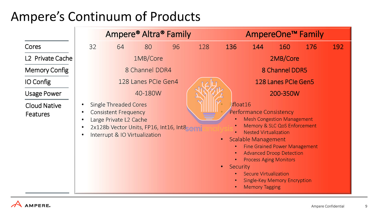
Moving on to today’s announcement, Ampere is continuing this journey with a new 192-core CPU with in-house CPU cores, up from 80/128 in the prior generation. Ampere moved to DDR5 memory and PCIe Gen 5, which massively improves IO throughput. In addition, Ampere has added a whole host of features to improve consistency and advanced fleet and lifecycle management features to assist cloud providers with deployments.
Mesh congestion – attempt to reroute communications between cores and from cores to memory or IO through alternative, less congested paths on the mesh.
Nested virtualization support – allows the tenants of cloud vendors to also run virtual machines inside their already virtualized environments with little to no performance impact.
Droop detection and process aging monitors – assist with managing the gradual breakdown of a chip as it is used and prevent instability.
Security – Features like secure virtualization, single-key memory encryption, and memory tagging enable tenants of a cloud to ensure their data is secure despite sharing memory controllers and sticks of DRAM. The features help prevent buffer overflow attacks and improve data integrity with databases.
The most interesting aspect of Ampere’s new design is its architecture. Ampere has moved to a chiplet-style architecture utilizing 5nm TSMC for the CPU cores and IO dies for memory controllers and PCIe controllers. The physical configuration is similar to that of Amazon’s Graviton3. It also uses AMBA CHI to connect to the chiplets.
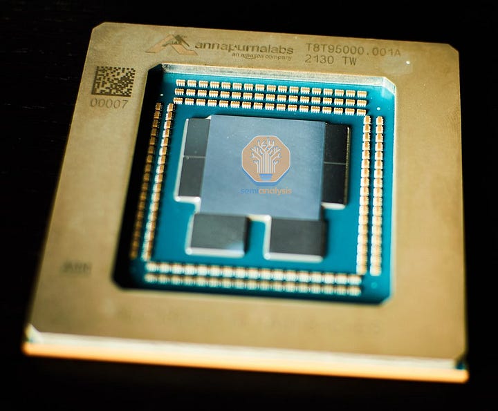
Ampere’s adoption of the chiplet style approach is one that enables them to make a new CPU core die and come with a refresh that has more than 192 cores next year.
We have done a mockup of the new AmpereOne A192 “Siryn” chiplet design using floorplans of Altra presented by the company at ISSCC 2022. Our mockup adopts the same chiplet layout as Graviton3, as both use a similar mesh and chiplet interconnect interface. Such a setup offers easy configurability and predictable performance over different sizes of VMs. CPU throughput of a 32-core VM would basically scale linearly compared to a 4-core VM. This is opposed to the chiplet design adopted by AMD, with multiple core chiplets surrounding a central IO die. Larger VMs that need to occupy multiple core chiplets suffer from performance inconsistencies compared to VMs that can stay in the same chiplet.
It is noteworthy that Ampere states they have been sampling this chip for a year, but is only now entering mass production. This suggests they needed to respin the chip a couple of times to get it right. While that is a pain, that isn’t as bad as the 12 respins and over 2.5 years that it took Intel to get Sapphire Rapids right.
Packaging & Thermal Design
Ampere’s current Altra line with its large, monolithic die and relatively tame power levels did not require sophisticated packaging and thermal design. The die sat atop a regular organic substrate (LGA 4926), with a polymer thermal interface material (pTIM) sitting between the die and a large integrated heat spreader (IHS) to dissipate heat.
This changes with AmpereOne. Gone is the IHS, with Ampere adopting a Direct Die contact design with a large, thick stiffener ring like what we see with GPUs and mobile CPUs. However, those are soldered BGA designs, whereas AmpereOne slots into LGA 5964 sockets. A direct die approach removes layers of thermal resistance by placing the cooler’s cold plate as close to the heat-producing silicon as possible, helping with temperatures.
As usage power skyrockets to 350W and even higher in peak power scenarios, the thermal design of the package is getting more scrutiny. Amazon also went from IHS to direct die in the move from Graviton2 to Graviton3. Meanwhile, the datacenter CPU incumbents (Intel, AMD) are sticking to conventional IHS with solder TIM for now.
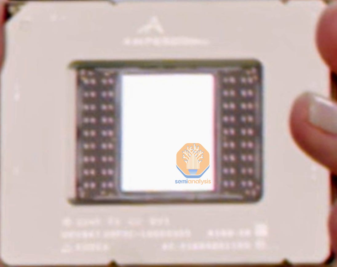
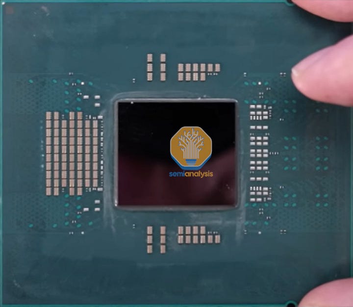
Although Ampere says Siryn is a chiplet design, a visual look at the package only shows a single large die. We reconcile this observation by proposing that what is visible is just a carrier wafer sitting atop all the chiplets. During the advanced packaging process, all the chiplets are bonded to a carrier wafer before being diced and attached to the substrate with a fine-pitch chiplet interconnect (InFO, CoWoS-R, FoCoS).
This structural silicon above the chiplets not only provides additional structural rigidity and durability required for a direct die design with 3rd party cooler mounting, but also serves as a silicon-based heat spreader to help even out thermal hotspots and spread heat from the hot core chiplet out across the cooler IO chiplets. As the material is the same as the compute and IO dies below, this minimizes Coefficient of Thermal Expansion (CTE) mismatch during repeated heating and cooling cycles, improving structural reliability.
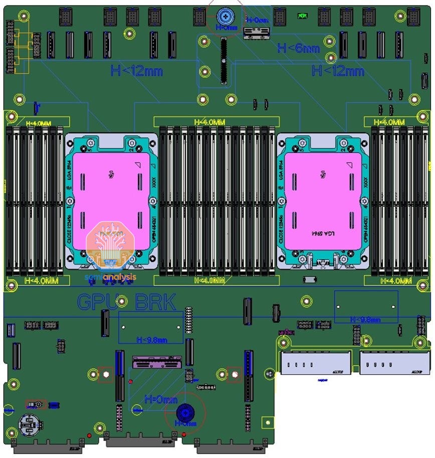
Although this top silicon prevents us from viewing the die size of the actual chiplets, it does show just how large the package is. The top die should be near reticle limit, meaning the package would be roughly 90mm x 70mm. This is larger than any currently available datacenter CPU. LGA 5964 board schematics of their Mt. Mitchell platform revealed at OCP Summit 2022 also show just how large the socket is.
In addition, Mt. Mitchell also offers a 12-channel DDR5 variant of AmpereOne which is in the works, providing 50% more memory bandwidth per socket.
This 12-channel variant would match AMD’s Genoa and Bergamo in memory bandwidth. It is also growing past 192-cores.
Performance – Disingenuous and Unfair Comparisons
Ampere never likes to talk about per-core or per-socket performance, instead preferring to stick to their metric of performance per rack. The majority of older datacenters are designed to power and cool about 14 to 20 kW per server rack. The racks vary in how many units they can hold but generally around 42 units (42U) with individual servers taking up 1U to 8U depending on the system architecture.
With CPU TDPs skyrocketing, these typical datacenter racks are now more power-constrained than space constrained. Stacking a rack full of high-density blade servers with high-power Xeons would blow out this power budget many times over, requiring specialized datacenter infrastructure with higher cooling capabilities. We also see this with Nvidia’s AI servers. Their DGX SuperPOD design is not able to fully populate each server rack due to the huge power consumption. Nvidia AI servers are often as much as 5U to 6U, with the A100 DGX servers being ~6.5 kW and the H100 10.2kW.
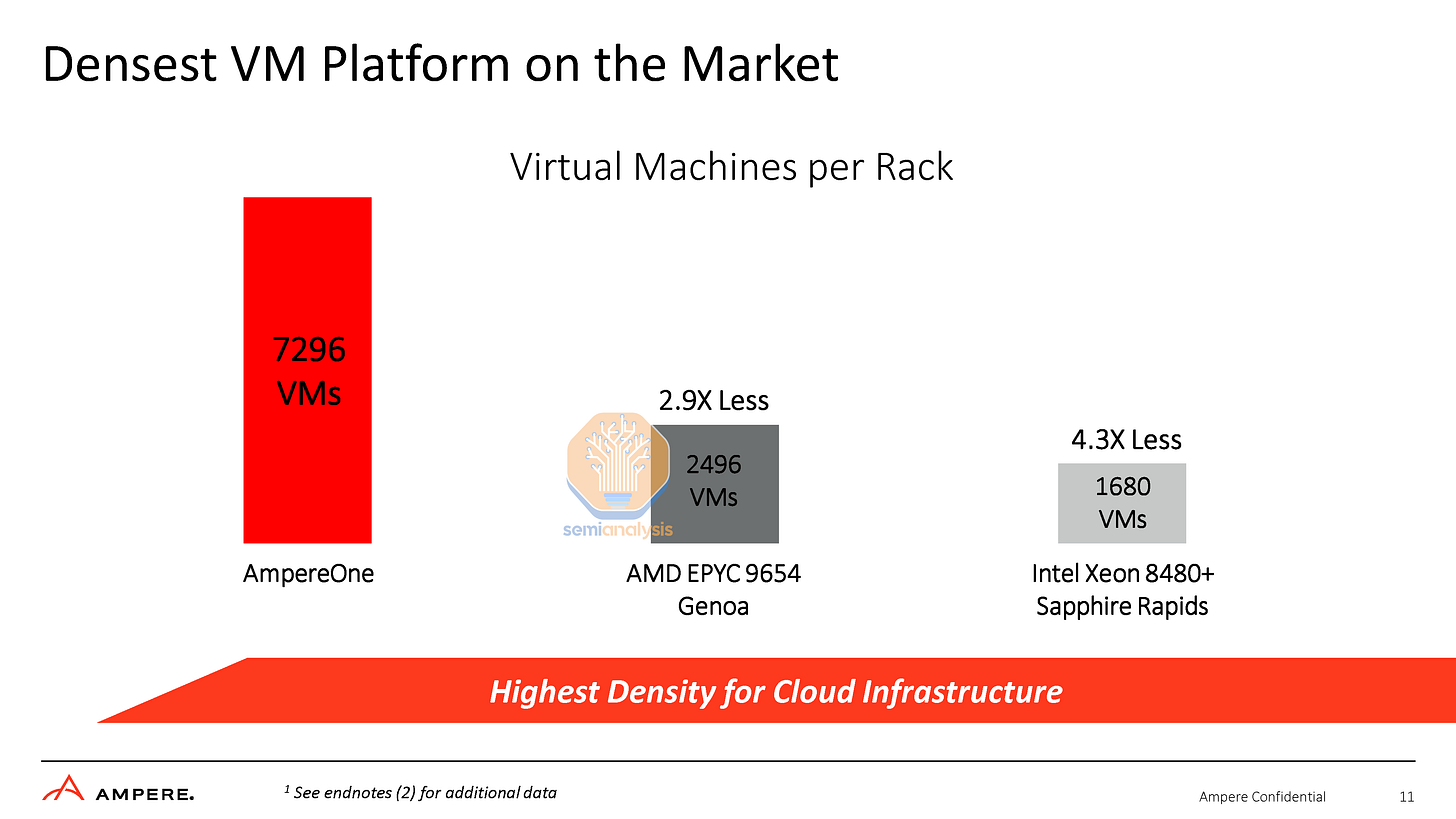
Ampere claims that in the industry standard SPEC CPU2017 Integer Rate workload, a single socket server of AmpereOne A192 draws 434W, AMD EPYC 9654 Genoa draws 624W, and Intel Xeon 8480+ Sapphire Rapids draws 534W. With a 16.5 kW power budget per rack, that means one rack can power 38 AmpereOne servers, 30 Intel servers or 26 AMD servers. Multiplying CPU cores per server with servers per rack, and assuming single-core VMs, we arrive at their claim of AmpereOne powering a whopping 2.92 times the VMs compared to the current best from the x86 world.
While this metric is useful for those seeking to cram as many VM clients per server rack as possible, it ignores the performance aspect, which is fine if clients just need a performance per core level that is ‘good enough’. We have extracted the submitted results of SPEC CPU2017 to show the stark difference in integer performance per core with the current Altras and CPUs on the market.
While AmpereOne should no doubt offer better Integer performance per core vs Altra, we do not see it coming anywhere close to AMD or Intel. Furthermore, CPUs from the competition are pushed out of the box for maximum performance per socket with high power consumption. One can always find a more efficient point in the performance/power curve by spending more and turning down power to fit more CPUs per rack.
Ampere did not disclose SPEC integer rate performance, but if we were to measure it as performance per rack, then AmpereOne would be much closer to the competition, especially with the upcoming 128-core Bergamo processor. Also, note the integer-weighted results of Ampere processors. The targeted cloud native workloads are primarily integer performance-focused, which is the polar opposite of HPC workloads where NVIDIA’s Grace Superchip should excel at.
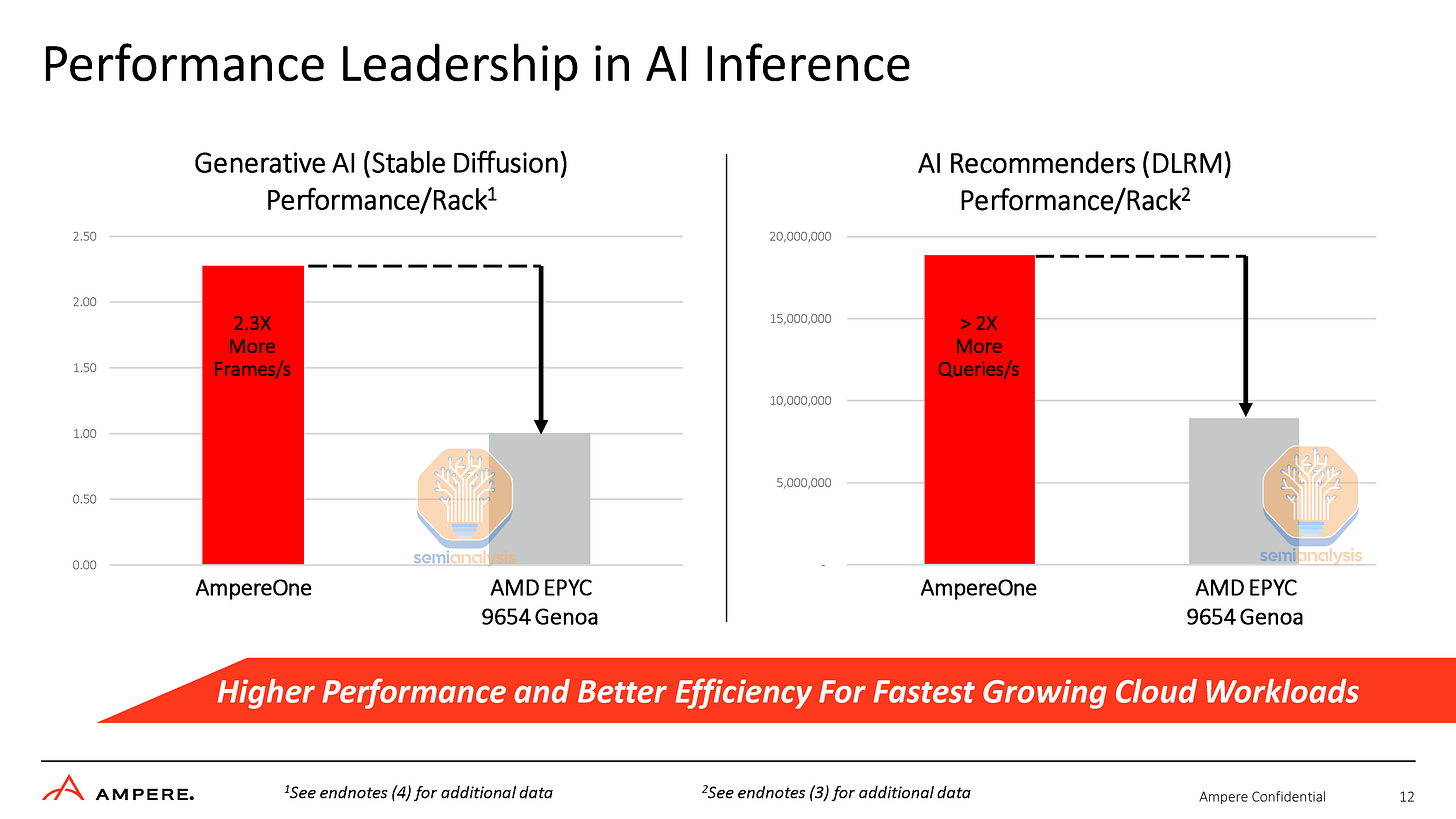
It is here where the comparisons get really unfair. In the Stable Diffusion test, AmpereOne is configured with 160 cores, 512GB of DDR5 and Linux kernel 6.1.10, while AMD’s Genoa is hamstrung with half the memory at 256GB and only populating 8 of its 12-channel memory capability, on an older 5.18.11 kernel. Furthermore, they only spawned 96 threads for Genoa, while they spawned 160 threads for AmpereOne. Genoa generally requires all 12 channels of memory and 192 threads (utilizing SMT) to achieve maximum performance.
The disingenuous settings don’t stop there. With the DLRM test, there was an additional difference in that AmpereOne used FP16 data formats while their AMD system was configured to use the FP32 data format. Higher precision data puts even greater memory pressure on these memory-bound AI workloads and hurts performance further.
This is really inexcusable as both processors support the reduced precision BF16 format, which could have been used. While we expect AmpereOne’s AI performance to be great, there is no need to fudge the setups to make the difference even greater. Shame on you Ampere.
Curiously, AmpereOne is shown to pull far more power in AI workloads than SPEC integer rate. While 192-cores in SPEC pulled 434W system power, 160-cores in Stable Diffusion pulled 534W. The opposite is shown for Genoa, pulling 624W in SPEC but only 484W in Stable Diffusion. This would indicate a performance optimization deficit between these processors. It would also indicate that Genoa could be underutilized due to Ampere’s tricks.
Core Microarchitecture
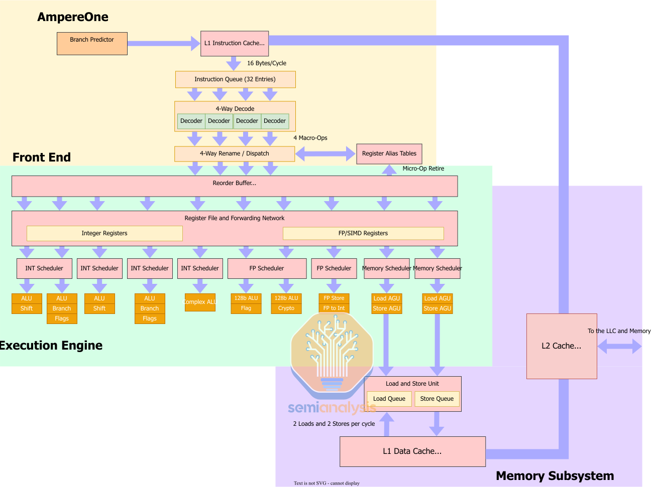
Ampere’s in-house core microarchitecture is an interesting mix of changes from their former Neoverse N1 core that they licensed from ARM Ltd. For one, they have increased the number of pipelines from 8 to 12 by adding a 5th Integer ALU, 2 more load/store AGUs, and a dedicated Floating Point store unit that can also do Float to Integer conversations. To deal with the added pipelines and execution units, Ampere reconfigured the scheduler layout from N1’s.
From the 8 independent schedulers on N1, AmpereOne has 8 schedulers, of which 4 are for the integer side, 2 for the floating point and vector units, and 2 for the memory side. Looking at the LLVM patches, this is what we think the scheduler layout looks like.
Moving to the rest of the core, AmpereOne has a re-order buffer (ROB) of a reported 174 entries which, while very small for a modern high-performance core, is a nice bump from the 128 entry ROB N1 had. This allows AmpereOne to get better instruction level parallelism compared to N1 and will let the core deal with more operations at any one time.
For the load and store system, Neoverse N1 was limited to either 2 128b loads or 1 128b load and 1 128b store. On AmpereOne, this is increased to 2 loads and 2 stores per cycle. Now we don’t know if the 2 loads and 2 stores also apply to 128b operations but we find it very likely that AmpereOne can do 2 128b loads and 2 128b stores per cycle, doubling the load and store bandwidth.
AmpereOne’s cache sub-system has seen some notable changes. The L1 data cache is the same 64 KB 4-way setup that Neoverse N1 has, and Ampere has doubled the L2 cache from the 1MB 8-way configuration to a 2MB 8-way configuration which helps with keeping data local to the core which is important for cloud workloads.
Ampere has also changed the L3 layout as well. Ampere has said that their 64MB “L3 cache” is more like Apple’s SLC in that it is a memory side cache instead of a more traditional L3 cache like AMD and Intel use. They have also said that they are using ARM’s CMN mesh but they haven’t commented much on the mesh layout beyond it having 64 distributed home nodes and directory-based snoop filters to enable seamless connectivity between the cores. How they are getting 64MB of LLC with 192 cores, we are unsure, and Ampere is giving no answers at this point. One way to arrange the L3 is to follow from what they did with Altra, where L3 is spread out across the mesh network, but not all mesh stops with 4-core clusters contain L3. The other way is for all L3 to be placed in large groups next to the DDR5 memory controllers, akin to other memory side caches like AMD’s Infinity Cache.
The real interesting change here is the reduction from a 64KB 4-way L1 instruction cache to a 16KB 4-way L1 instruction cache. This is an interesting move that I don’t know will be beneficial for performance. Now traditionally, a bigger L1 instruction cache (L1i) is traditionally considered better because staying in the caches closest to the core is much more power efficient then going out to higher level caches, like the L2 cache, as well as being higher bandwidth.
On the latter point of the L1 being higher bandwidth than the L2, this is likely not the case with AmpereOne. Now we don’t know the bandwidth of either the L1i cache or the bandwidth between the L2 and the L1i, but it is likely that bandwidth from the L1i to the rest of the core is 16 bytes per cycle. Most ARM instructions are 4 bytes in length and AmpereOne has 4 wide decode. So, to keep the core fully fed with new instructions, AmpereOne likely has a fetch bandwidth of 16 bytes per cycle. The L2 cache also likely has a 16 byte per cycle link to the L1i because a 16 byte per cycle link to the L1i is quite common in modern CPU cores.
But as for the former point, we don’t know why Ampere chose to cut the L1i but there are at least 2 reasons we can think of. The reduction in the L1i is for area saving because L1i uses very un-dense SRAM with high accessibility so cutting it to 16KB could save a lot of area. The other reason is that the workloads they profiled get significantly less performance as you go from 16KB to 32KB to 64KB such as SPEC INT 2017 which isn’t super heavy on the instruction side.
Now, we suspect that it’s likely a combination of these factors along with other pressures that had Ampere go this direction. However, this is a cloud processor so while they may have workloads that they are focusing on this also has to be a CPU core that is good enough for general-purpose workloads.
IPO, Hyperscale In-house Chips, and AMD/Intel Competition
Next we want to discuss the IPO, long-term prospects with increased competition, AMD/Intel’s response, the RISC-V ecosystem, and in-house roadmaps from hyperscalers such as Amazon, Google, Microsoft, and Alibaba.


