Tesla AI Capacity Expansion – H100, Dojo D1, D2, HW 4.0, X.AI, Cloud Service Provider
Tesla has aspirations of being a top 5 AI company in capacity and a cloud service provider
Tesla has aspirations of being one of the leading AI firms in the world. To date, they do not have the most advanced self-driving deployed; that honor applies to Alphabet’s Waymo. Furthermore, Tesla is nowhere to be seen in the generative AI world. With that said, they potentially have the recipe to leapfrog in autonomous vehicles and robotics due to data collection superiority, specialized compute, innovative culture, and leading AI researchers.
Tesla currently has a very small amount of AI infrastructure in-house, with only ~4k V100s and ~16k A100s. Compared to the other large tech companies of the world, this is a very small number, given firms like Microsoft and Meta have 100k+ GPUs, and they look to double those numbers over the short to medium term. Tesla’s weak AI infrastructure is partially due to multiple delays with their in-house D1 training chip.
Now the story is changing, and quickly.
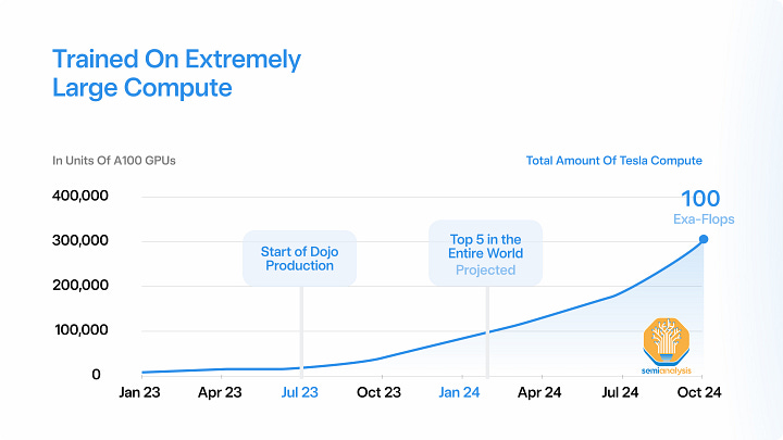
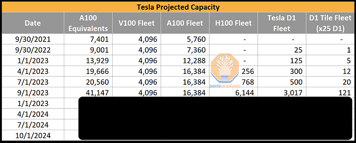
Tesla is massively increasing it’s AI capacity by a factor of more than 10x in 1.5 years. Part of this is for their own capabilities, but a large portion is also for X.AI. Today we want to dive into our Tesla’s AI capacity, H100, and Dojo ramp’s by quarter with unit estimates, and the unique needs of Tesla due to their model architecture, training infrastructure, and edge inference including HW 4.0. Lastly, we want to discuss what X.AI is doing, Elon’s competitor to OpenAI which has poached a number of notable engineers from OpenAI.
The story of the D1 training chip is a long and arduous one. It’s faced issues from silicon design to power delivery, but now Tesla claims it is ready for the limelight and started volume production. For a bit of a refresher, Tesla has been designing in-house AI silicon for their cars since ~2016 and for datacenter applications since ~2018. We exclusively disclosed the special packaging technology they utilize before the chip was announced. That technology is called InFO SoW. For simplicities sake, think of it as a fan-out package the size of a wafer. This is similar to what Cerebras does in principle, but with the advantage of allowing known good die testing. It is the most unique and interesting aspect of Tesla’s architecture as 25 chips are built into this InFO-SoW with no memory directly attached.
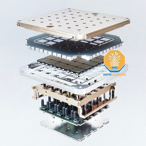
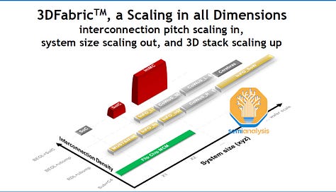
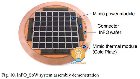

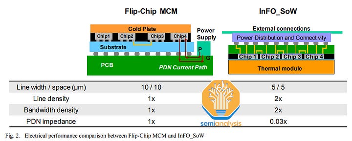
We also discussed both the pro’s and con’s of their chip architecture in more detail back in 2021. The most interesting aspect since is that disclosure is Tesla had to make another chip that sits on a PCIe card to provide memory connectivity as on-chip memory was not enough.
Tesla was supposed to ramp multiple times in 2022, but never did so due to silicon and system issues. We are now in mid-2023, and it is finally ramping up production. The architecture is great for Tesla’s unique use case, but it is noteworthy it is not useful for LLMs which are heavily memory bandwidth bottlenecked.
Tesla’s use case is unique because it must focus on image networks. As such, their architecture differs greatly. In the past, we have discussed how deep learning recommendation networks and transformer-based language models require very different architectures. Image/video recognition networks also require a different mix of compute, on-chip communications, on-chip memory, and off-chip memory requirements.
These convolutional models, during training, achieve very poor utilization on GPUs. With Nvidia’s next generation running headlong into further optimizations for transformers, especially sparse MoE, Tesla’s investment in their own differentiated, optimized architecture for convolutions, should play out well. These image networks must fit within the constraints of Tesla’s inference infrastructure.
Tesla HW 4.0, Second Generation FSD Chip
While the training chips are made with TSMC, the chip that runs AI inference inside Tesla EVs is called Full Self-Driving (FSD) Chip. Tesla’s models on their vehicles are extremely limited as Tesla has a very stubborn belief that they don’t need huge performance in the car to achieve full self-driving. Furthermore, Tesla has much more stringent cost constraints than Waymo and Cruise because they actually ship large volumes. Meanwhile, Alphabet Waymo and GM Cruise are using full-sized GPUs that cost 10x more in their cars during development and early testing and are looking to make their own much faster (and more expensive) SoCs for their vehicles.
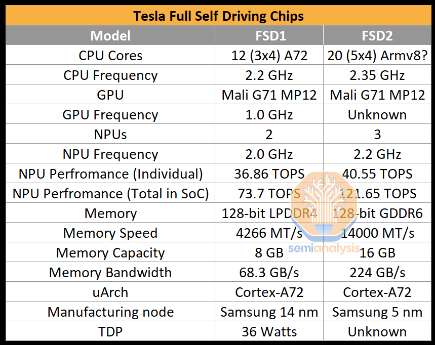
The second-generation has been shipping in cars since February of 2023, the chip represents a very similar design to the first-generation design. The first generation was based on Samsung’s 14nm process and was built around three quad-core clusters, for a total of 12 Arm Cortex-A72 cores running at 2.2 GHz. However, with the second-generation design, the company bumped up the CPU core count to five clusters of 4 cores (20), for a total of 20 Cortex-A72 cores.
The most important part of the second-generation FSD chip is three NPU cores. The three cores use 32 MiB of SRAM each for storing model weights and activations. Each cycle, 256 bytes of activation data and 128 bytes of weight data are read from the SRAM to the Multiply Accumulate units (MACs). The MACs design is a grid, with each NPU core having a 96x96 grid for a total of 9,216 MACs and 18,432 operations per clock cycle. With three NPUs per chip running at 2.2 GHz frequency, the total compute power is 121.651 trillion operations per second (TOPS).
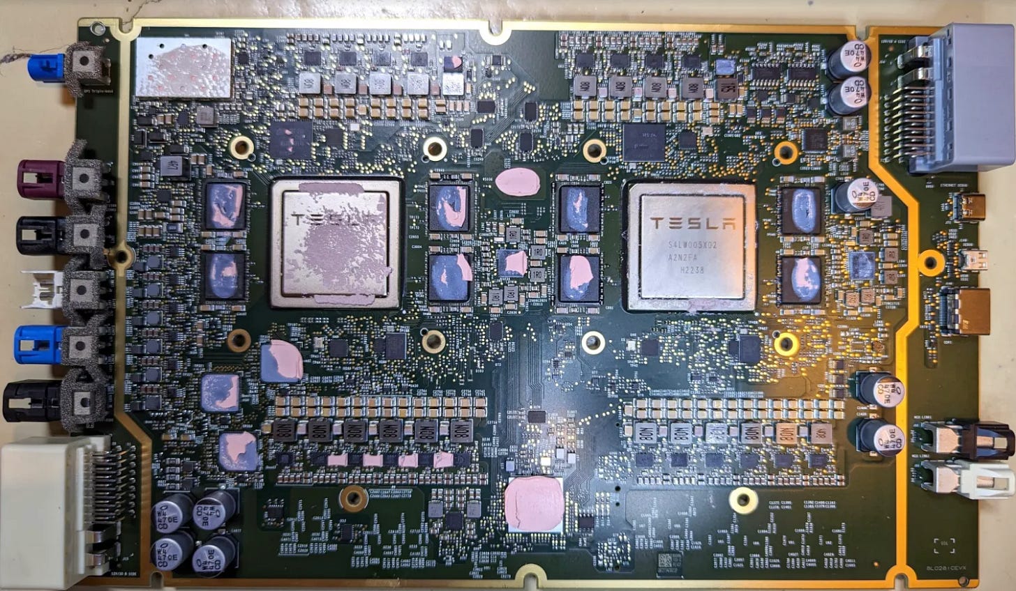
The second generation FSD has 256GB of NVMe storage and 16GB Micron GDDR6 at 14Gbps sitting on 128-bit memory bus providing 224GB/s bandwidth. The latter is the most noteworthy change as bandwidth has gone up ~3.3x gen on gen. The increase in FLOPs vs bandwidth indicates that HW3 had difficulty being fully utilized. There are two FSD chips per HW 4.0.
The increased performance of the HW4 board comes at the expense of additional power usage. The idle power consumption of the HW4 board is about double compared to the HW3. At peak, we expect it to be higher as well. The external HW4 housing notes 16 Volts at 10 Amps, translating into 160 Watts of power used.
Despite the performance increases with HW4, Tesla wants to enable HW3 to achieve FSD as well, likely because they do not want to retrofit existing HW3 users who purchased FSD.
The infotainment system utilizes an AMD GPU/APU. That is also now on the same board as the FSD chips, compared to the last generation, which had a separate daughterboard.
The HW4 platform has support for 12 cameras, one of which is used for redundancy purposes, so 11 cameras are in active use. In the old setup, the front camera hub used three lower-resolution 1.2-megapixel cameras. The new platform uses two higher-resolution 5-megapixel cameras.
Tesla currently does not use LIDAR sensors or other types of non-camera approaches. In the past, they did utilize radar, but that was removed mid-generation. This significantly reduced the cost of manufacturing a vehicle, which Tesla was lasered in on optimizing, and the company believes that pure camera sensing is a possible route to self-driving vehicles. However, they also noted that if a viable radar is available, they will integrate that with the camera system.
In the HW4 platform, there is an in-house designed radar coming called Phoenix. Phoenix combines a radar system with a camera system aimed to create a safer vehicle by utilizing more data. The Phoenix radar uses the 76-77 GHz spectrum with 4.16 Watts at peak Effective Isotropic Radiated Power (EIPR) and 177.4 mW average EIRP. It is a non-pulsed automotive radar system with three sensing modes. The radar PCB includes a Xilinx Zynq XA7Z020 FPGA for sensor fusion.
Tesla AI Models Differentiation
Tesla aims to produce foundational AI models to power its autonomous robots and cars. Both need to be aware of their surroundings and navigate around them, so the same type of AI models can be applied to both. Creating efficient models for future autonomous platforms requires a lot of research, and, more specifically, a lot of data. Furthermore, inference of these models must be done at extremely low power and low latency. This dramatically reduces the maximum model size Tesla can offer due to their hardware restraints.
Out of all companies, Tesla has the biggest dataset available for training of its deep learning neural networks. Each vehicle on the road uses sensors and images to capture the data, and multiplying that by the number of Tesla EVs on the road yields a massive dataset. Tesla calls its part of collecting data “fleet scale auto labeling”. Each Tesla EV takes a clip – 45-60 second log of dense sensor data, including video, inertial measurement unit (IMU) data, GPS, odometry, etc., and sends it to Tesla’s training servers.
Tesla’s model are trained on segmentation, masks, depth, point matching, and other tasks. By having millions of EVs on the road, Tesla has a large selection of data sources that are very well-labeled and documented. This enables continuous training in the Dojo supercomputer at the company’s facility.
Tesla’s beliefs on data contradict the available infrastructure that the company has built. Tesla uses only a tiny fraction of the data they collect. Tesla is famous for overtraining their models to achieve the best possible accuracy within a given model size due to their tight inference limitations.
Overtraining small models leads to a plateau of performance for full self-driving, and an inability to use all the data gathered. Many companies are likewise choosing to do training on as large of a scale as possible, but they are also using car inference chips that are much more powerful. For example, Nvidia plans to deliver DRIVE Thor with over 2,000 TeraFLOPS of compute power to automotive customers in 2025, that’s more than 15x what Tesla’s new HW4 can do. Furthermore, the Nvidia architecture is more flexible to other model types.


