We try to stay fact based with our analysis, but recently an image was posted of a Tesla chip that leads to an immense amount of speculation that we would like to dip out toes in. It was posted by Dennis Hong, a world-renowned researcher for robotics and autonomous driving. He is a professor and runs a large lab at UCLA. His tweet only states Tesla AI Day alongside the date of August 19th, time, and location of the event. The timing is quite interesting considering Tesla just built what could be considered by some, the world’s 3rd largest supercomputer. That was built with Nvidia GPUs using Super Micro Systems.
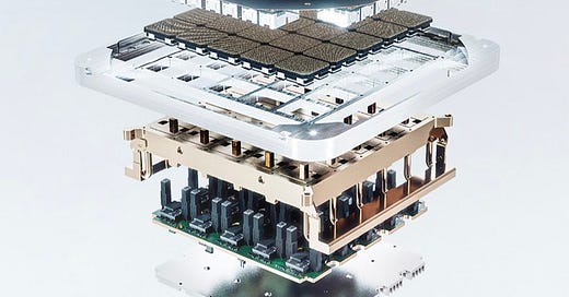
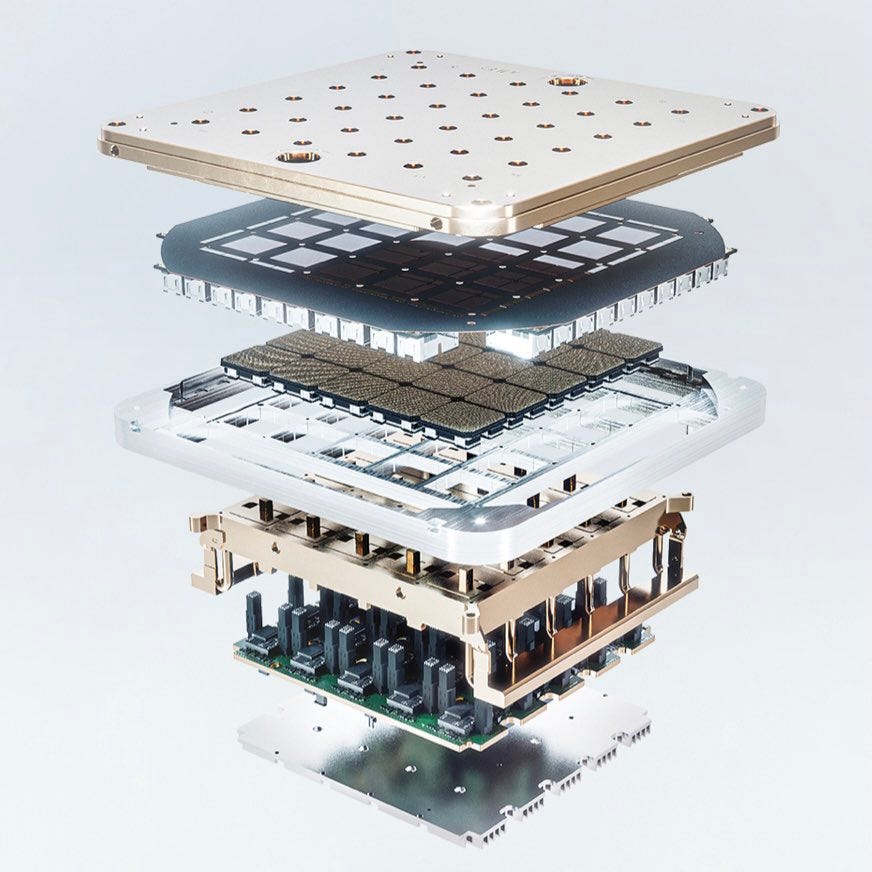
At first glance it looks like there is a carrier, heatsink, and power delivery. The most interesting part of course, is the chips. It has a large array of BGA solder pads and a 5x5 array of chips. This type of packaging looks incredibly unorthodox and the only thing we can think of is TSMC’s integrated fan out system on wafer technology (InFO_SoW). Here is the link to the paper on IEEE.
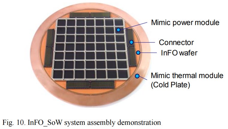
This image looks remarkably similar to the Tesla chip and offers some insights. Just like the tesla image, there is a cold plate. Various chips arrange in a grid, an InFo Wafer, and connectors. The structures look to be a 1 to 1 match but the exact details them look to be slightly different than the initial TSMC research.
InFO_SoW eliminates the use of substrate and PCB by serving as the carrier itself. Close packed multiple chips arrays within a compact system enable the solution to reap the wafer-scale benefits such as low latency chipto-chip communication, high bandwidth density and low PDN impedance for greater computing performance and power efficiency. In addition to heterogeneous chips integration, its wafer-field processing capability has enabled chiplet-based design for greater cost saving and design flexibility.
This breaks through the current barriers with multi-chip modules. With an interposer-based technology such as Nvidia datacenter GPUs, they are limited by interposer manufacturing limits. TSMC’s 5th generation CoWoS-S recently went into mass production with interposers that are 3x the reticle limit. The reticle limit is 26mm by 33mm and is associated with the maximum area a lithographic machine can pattern in one instance. This method involves reticle stitching and other manufacturing difficulties because the interposer is a silicon chip itself. This type of packaging has limitations in scaling the number of chips for huge AI workloads.
The other method is with flip chip packaging. The most well-known MCM design with this type of packaging is AMD CPUs. They do not have the issues with reticle limits, but there are huge drawbacks in terms of power and wire density. You burn significantly more power on inter chip data transfers and the bandwidth between chips is limited. This type of packaging would not suit well to huge AI workloads because of these limitations.
With the scaling that Tesla may hope to achieve in their Dojo supercomputer design, there will be an immense amount of heat. InFO_SoW is capable of 7,000W of power. This is compared to Nvidia’s datacenter A100 GPU which comes in configurations as high as 500W. With this requires immense consideration for cooling, and the TSMC paper on InFO_SoW offers a solution.
This image is quite crude, but the cold plate in the Tesla image looks similar in that it has many inlets and outlets. Water-cooling is a necessity with this level of power and heat density.
One other striking element is that there doesn’t seem to be any HBM or other DRAM based technology. Much like Cerebras, they are likely utilizing a design that relies entirely on-die SRAM. Check out our deep dive into the exact architecture utilized here.
While we are excited to see what happens at Tesla AI Day on August 19th, we won’t get too carried away on the exact specifics of this chip. InFO_SoW is just speculation despite some previous rumors stating a Tesla, Broadcom, TSMC partnership on productizing it. Google has a similar arrangement with Broadcom for the TPU line of AI accelerators. The combination of system on wafer technology with integrated fan outs could allow them to achieve amazing scale up AI performance that current AI accelerators from Nvidia and others can only dream of.
Samsung is almost certainly producing the next chip that is implemented in the cars themselves on their “5nm” node. This looks like it could be an entirely different chip that is larger and packaged in a very different manner. The image above would not be capable of going into mass produced automobiles, but rather in datacenters for training huge AI networks that are then used in the cars for self-driving.
This article was originally published on SemiAnalysis on August 4th 2021.
Clients and employees of SemiAnalysis may hold positions in companies referenced in this article.


