The fundamental component of any chip is the transistor, which recently celebrated its 75th birthday. Today we will discuss the next 25 years. Transistors are essentially switches for electrical current; a voltage that is applied to its “gate” can cause a current to flow in the channel between its “source” and “drain.” Each transistor can turn on or off, corresponding to a “1” or “0.” Driven by Moore’s Law scaling and improvements in CMOS process technology, modern computing chips do this on the scale of billions and even trillions.
An ideal transistor does the following:
Conducts the maximum amount of current when turned on
Doesn’t allow any current to flow when turned off
Switches as quickly as possible.
The 3 main components of a transistor: “gate,” “source,” and “drain”
A Brief History of the Transistor
Invented in 1947 at AT&T’s Bell Labs by John Bardeen, William Shockley, and Walter Brattain, the first transistors were known as “planar” transistors because all elements of the transistor, including the gate, source, and drain were situated on a two-dimensional plane.
For many generations, the switching speed of planar transistors could be increased by shrinking the gate length. “Straining” the silicon channel also increases the switching speed. To strain channels, a layer of silicon is placed over a layer of silicon-germanium (SiGe). As the atoms in the silicon layer align with the SiGe layer, this leads to the links between the silicon atoms stretching, thereby straining the channel. In this configuration, where silicon atoms are further apart, atomic forces that interfere with electron movement are reduced. The electron mobility (i.e., how quickly an electron can move when pulled by an electric field) improves by 70% in strained channels, leading to transistor switching speed increasing by 35%.
A further development that allowed for continued scaling was the development of “High-K/Metal” gates. At the 45nm node, the gate dielectric began to lose its insulating (dielectric) quality and exhibited too much leakage current (i.e., significant current would flow across a transistor when in its off state).
The gate dielectric is a very thin insulation layer, traditionally made of silicon dioxide, that lies between the transistor’s metal gate electrode and the channel through which the current flows. Intel made a significant breakthrough in its 45 nm process (2007) by using a hafnium-based dielectric layer with a gate electrode composed of alternative metal materials. The rest of the industry followed 3 years later. The resulting combination yields a “high dielectric constant” or “high K” gate.
As the transistor’s dimensions continued to decrease, the space between the source and drain decreased to the point where the gate lost the ability to properly control the flow of current in the channel. Because of this, planar transistors displayed significant “short channel” effects, especially below the 28nm node, where leakage current was excessive.
To address this challenge, the industry shifted to “3D” transistors, known as FinFETs.
In the FinFET, the gate wraps around the channel on three sides of a silicon fin, as opposed to just its top as in planar transistors. This allows for greater control of the current that flows through the transistor; FinFET transistors have significantly faster switching times than planar transistors. In the early 2010s, Intel moved into production with FinFET at the 22nm node, and foundries like TSMC ramped up the FinFET at 16nm 3 years later.
Due to the limit of how thin/high fins can be made as well as how many fins can be placed side by side, another evolution of the transistor is currently underway in the industry. These next-generation transistors are known as “Gate-All-Around” transistors, or GAAFETs. GAA uses stacked horizontal “nanosheets”, so that the gate surrounds the channel on all 4 sides. This increases the drive current and overall performance of transistors even further. The width of each nanosheet, as well the number of nanosheets in each transistor can be varied, allowing for custom designs.
In 2022, Samsung began using GAA in its 3nm process. Due to issues with yield, high-volume chips from Samsung’s 3nm GAP are expected in 2024. Intel has GAA on its roadmap with 20A process node which is manufacturing-ready in 2024 with products shipping in volume in 2025. TSMC has GAA with their N2 process node in 2025 or 2026. These production years are targets, and in our opinion, further delays from at least 2 of these players are likely.
Beyond initial GAA processes include moving to forksheet or 3D complementary FET (CFET), in which the n and p channel are moved closer together or stacked vertically.
To continue roadmaps beyond 2nm, the transition to Gate-All-Around will also require new transistor channel materials for the nanosheets. This is because the electron mobility in bulk materials like silicon and germanium drops significantly < 5nm. As we go deeper into the nanoscale, atomic effects can no longer be ignored. Perhaps the best family of materials to address these challenges is 2D materials.
2D Materials
2D materials are crystalline solids consisting of a single layer of atoms. The most well-known 2D material is Graphene, an allotrope of carbon consisting of a single layer of atoms arranged in a hexagonal lattice. However, it is important to note that graphene does not have a bandgap.
Semiconductors are defined by their band gap: the energy required to excite an electron stuck in the valance band, where it can’t conduct electricity, to the conduction band, where it can. The band gap needs to be large enough so that there is a clear contrast between a transistor’s on and off states, and so that it can process information without generating errors. Despite its high electron mobility, without a bandgap, graphene can’t be used as a semiconductor material. Although graphene has a bandgap when doped, doped graphene does not allow for sufficiently low off-currents or high on-currents.
The most promising 2D materials for next-gen nanosheets come from the “Transition Metal Dichalcogenide” or “TMD” sub-family. Materials from this group include Molybdenum disulfide (MoS2), Tungsten disulfide (WS2), and Tungsten Diselenide (WSe2). TMDs have the desired combination of bandgap + mobility required for < 5nm channel thicknesses.
This was highlighted by H.-S. Philip Wong in his HotChips 2019 Keynote, “What will the next node offer us?”
While Carbon Nanotubes (CNTs, which are 1-dimensional materials) were also highlighted, they remain notoriously difficult to manufacture after 30+ years of R&D. To achieve the desired performance metrics for transistor applications, millions of individual tubes have to be grown (i.e., density) and all aligned the same way (i.e., alignment). Also, with CNTs, you’re only dealing with Carbon. 2D materials are far more versatile, referring to an entire family of materials, and in theory, are easier to manufacture than CNTs. Large-area monolayer sheets can be grown and then transferred.
2D Material Growth
2D materials are often grown via Chemical Vapor Deposition (CVD), though more recent efforts also include Atomic Layer Deposition (ALD). Depending on the choice of substrate and parameters, 2D film growth can be monolayer or multilayer.
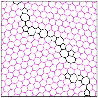
Monolayer graphene (the most mature 2D material), for example, is grown via CVD primarily on copper foil or film substrates today. However, current CVD growth techniques yield “polycrystalline” graphene with several grain boundaries in the crystal lattice. Growth is also variable, meaning that wafer-to-wafer consistency is difficult to achieve. With grain boundaries and other defects, intrinsic CVD graphene electron mobility is often still well under 10,000 cm2/(V⋅s), a far cry from the 200,000 cm2/(V⋅s) value reported for pristine, exfoliated graphene flakes at a carrier density of 1012 cm−2.
Exfoliated graphene refers to pure flakes of graphene delaminated from graphite; this is how graphene was first isolated in 2004 when two researchers from the University of Manchester (Andre Geim and Kostya Novoselov) used scotch tape to peel of layers of graphene from graphite.
As you can imagine, when you have a material/wafer where properties vary so wildly, metrology/inspection becomes incredibly difficult.
As such, the graphene electronics market is negligible today, with a few players mainly focused on sensors (ex: hall effect) or mems devices (less restrictive lithography rules/larger line widths, higher variability can be tolerated etc.). Companies like Cardea Bio and GrapheneDX are working on graphene biosensors in particular, as graphene is biocompatible and can be functionalized to detect various molecular compounds via Field Effect Sensing. Other companies like Graphenea and Applied Nanolayers, both in Europe, are building dedicated graphene foundries.
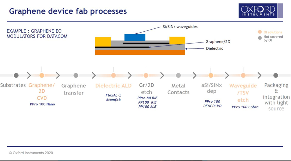
TMDs like MoS2 and WS2 are even more nascent and are often grown on sapphire wafers today. Aixtron and Oxford Instruments are currently the only OEMs selling dedicated growth tools for 2D materials. For 2D materials to be taken seriously, a more consistent wafer-to-wafer growth process has to be developed, with the goal of achieving “single crystal” materials long term.
2D Material Transfer
Since 2D growth is often done at higher temperatures (>600° C) on optimized substrates like copper or sapphire, a transfer step is required to move the 2D material to the final silicon wafer.
Current methods to transfer 2D materials from their growth substrates to target silicon device wafers are insufficient for the CMOS market (requiring some combination of wet chemistry/etchants, metal deposition, sacrificial polymer layers, thermal release tape [TRT] which leaves behind residue, and/or laser debonding). The most conventional 2D transfer technique involves wet etching the copper substrate and using the polymer polymethyl methacrylate (PMMA) to pick up and move the 2D material to a target substrate. However, PMMA residue remains on the graphene surface after transfer and degrades the electrical properties of graphene.
Today’s 2D material transfer methods are sufficient for some applications/devices like sensors or “roll-to-roll” / displays, but do not clear the bar for CMOS in terms of quality, throughput, and contamination.
Direct Growth vs. Transfer
While direct growth of 2D materials on silicon is preferred, thus far, it has been difficult to achieve a low-temperature, high-quality growth solution. While ALD allows for lower temperatures than conventional metalorganic CVD or MOCVD, throughput remains slow.
It is perhaps better to decouple a slower, high-quality growth step on an optimized substrate from a high throughput, optimized transfer step. This will allow for better process optimization and yield control. This may be best when dealing with expensive < 2nm, High-NA EUV + GAA wafers at the leading edge (especially if multiple nanosheets are needed per transistor).
Decoupling is also fab-friendly as growth and transfer can be done asynchronously to ensure maximum fab process line utilization rates (enabling higher WPH numbers).
Lastly, the transfer is more versatile, allowing for heterostructure, stacked, and twisted configurations more easily than direct growth. This has the potential of opening up the field of 2D twistronics longer term.
IEDM 2D Highlights
The 68th annual IEDM meeting in San Francisco offered a great perspective on the future of the semiconductor and computing industries. Notable amongst the industry leaders’ presentations in attendance was Intel’s commemorating 75 years of the transistor, which presented both a look at the past and a vision for what may lie ahead.
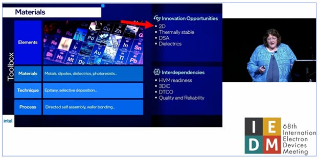
As Moore’s law slows down, novel technologies drive performance gains, whether it’s a post-silicon channel world or packaging technologies. Intel’s presentation suggested three areas that might drive the industry and scaling targets forward: novel dielectrics, directed self-assembly (for nanopatterning), and 2D materials.
2D materials, in particular, made an outsized appearance at the conference. The industry has a clear roadmap for the near future, with the FinFET and GAA architecture extending the silicon channel’s reign. What happens beyond that is more challenging and nebulous. Notably, Intel demonstrated a 2D material channel in a GAA structure with low leakage and near-ideal switching, an important step towards stacking transistors vertically. IMEC’s roadmap introduces the complementary FET (CFET) as a similar solution, in which the n and p channels, based on monolayer transition metal dichalcogenides (TMDs) such as WS2 or MoS2 are stacked.
At IEDM, there was a specific session for 2D Channel Technology, co-chaired by Dr. Eric Pop from Stanford University and Nicolas Loubet from IBM’s Advanced CMOS Logic Program.
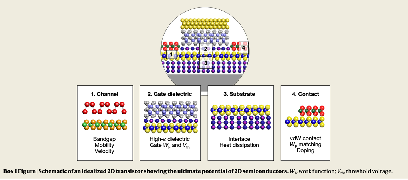
Papers/presentations focused on various aspects of 2D transistors, including the channel, gate dielectric, substrates/materials required, and lowering contact resistance to increase device performance. What follows is a technical review of some of these papers:
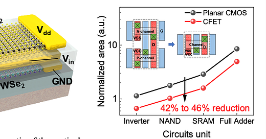
Amongst the developments presented was research by Peking University in China, illustrating top gated CVD grown WSe2 pFETs with a drain current of 594 uA/um, in addition to a WSe2/MoS2 based CFET1. The CFET structure, when compared to traditional planar ICs showed an 8% improvement in performance in addition to a 44% reduction in area. A number of challenges remain, mostly in manufacturability. The CFET demonstrated in this paper was nearly manufactured in a fab-compatible manner, with the exception of a wet transfer technique used for the MoS2 channel in the nFET. Scalable dry transfer techniques will be critical to moving such technology to production.
2D CFET Structure and Integration Area Reduction. Vertical stacking can lead to much higher-density components without performance loss.1
An R&D challenge in this vertical stacking approach is largely in placing the source and drain contacts and choosing contact materials for interconnects. TSMC, in another IEDM paper, provided insight into ideal materials for this purpose in transferred MoSe2 channel devices on SiN2. The challenge of choosing contact materials lies in finding a combination of ideal work function and weaker Fermi level pinning effects; TSMC chose to utilize a thin layer of antimony (Sb) and high work function platinum (Pt) to achieve this goal in nFETs and pFETs with WSe2 channels. This contact engineering effort resulted in lowest reported contact resistances, with 0.75 kΩ-um for the pFET and 1.8 kΩ-um in the nFET. In the nFET, this represents a 72% reduction in contact resistance from previously reported values, representing a large step forward to the advancement of the 2D channel for logic applications.
Contact resistance is merely one component of the total resistance of a device; spacer resistance is another major contributor to poor device performance, particularly in pFETs. TSMC, in another IEDM paper, utilized WOx formed by oxidizing multilayer WSe2 in conjunction with a WSe2 channel as a low-resistance spacer dopant3. WOx serving as a high p dopant, was found to lower the Schottky barrier height, leading to lower total resistances despite the addition of the dopant (1 kΩ-um).
pFET with WOx dopant formed by oxidizing multilayer WSe2.3
While TMD-based devices are promising, there is a fundamental issue on TMD growth methods. Transfer-based methods leave polymer residues, while direct growth on oxide with MOCVD results in a variety of defects, most notably organic contaminants and sulfur vacancies. IEDM featured a number of papers using both methods, transfer, and direct growth.
Intel featured a 2D FET based on transferred MoS2 with a source-to-drain contact length of 25 nm, comparable with current silicon process nodes. The tested devices showed an uptick in subthreshold swing (SSsat= 75 mV/dec) below a source-drain distance of 34 nm. However, Intel’s process used a layer transfer process using an ALD-grown sacrificial dielectric layer, which left significant amounts of residue and led to MoS2 delamination at both the source and drain contacts. For manufacturing and future yield goals, transfer methods must be made residue-free and dry, or feature direct growth methods.
Direct growth advances were also discussed, with more fab-compatible processes utilizing CVD observed. A paper from Peking University discussed a WSe2 pFET with low contact resistance (0.65 kΩ-μm) that is purely Ohmic5. The device, with a channel length of 120 nm, posted record performance numbers (Ids= 425μA/μm, gm=80μS/μm, SSsat=200 mV/dec) when grown on 6nm of SiO2. This process was also compatible with growth onto a Si/HfLaO dielectric film, while posting slightly worse performance (Ids=370μA/μm, gm=100μS/μm, SSsat=250 mV/dec). However, the high processing temperature of growth (890° C) in the first device’s fabrication poses a fab compatibility risk for manufacturability. However, this work does represent a sizeable advancement of p-type 2D TMD materials, which is an area within 2D materials in need of development.
2D materials were also featured in dielectric interface engineering for MoS2 transistors using hBN as an encapsulation layer6. This work resulted in the lowest reported subthreshold swing for CVD-grown monolayer MoS2 devices. The encapsulation layer also seemed to improve device reliability, showing less off-state degradation after Al-seeding and top gate deposition, suggesting that the dielectric layer minimized damage from further processing. This represents an advancement in 2D-material-based device reliability and lifetimes. When using a tantalum (Ta) seeding layer for a TaOx doping layer, a large Ids= 861μA/μm and a low subthreshold swing (72 mV/dec) are reported, while for low power applications, a high Ids=598 μA/μm and Vds=0.65 V are reported, exceeding IRDS 2028 HD specifications.
The 2D advances discussed represent but a mere slice of the potential of 2D materials to revolutionize the industry. However, significant challenges remain to translate 2D to high-volume manufacturing at the fab level. All of the above papers utilize wet transfer techniques to move 2D materials from growth substrates to production wafer. While promising to illustrate device potential, as seen above, this approach is not scalable to high-volume manufacturing due to the potential for polymer residue and lower throughput. Nevertheless, with every IEDM conference, the path forward for the semiconductor industry becomes clearer: 2D is the future, and in the view of these authors, inevitable. As of now, the leading-edge community seems to favor WS2 and WSe2, because they can be made both n-type and p-type.
2D materials are clearly the future of the industry, with a lot of momentum pushing the field forward. As 2D materials move into semiconductor stacks, the development of tools to effectively characterize them inline will also be needed. To this end, upcoming talks at SPIE Lithography and Patterning conference discuss the outlook in metrology as well as growth in talks by Intel and IMEC:
Are 2D transition metal dichalcogenides transistors the future silicon replacement or hype?
300mm in-line metrologies for the characterization of an ultra-thin layer of 2D materials
In addition, IMEC, which is spearheading the EU Graphene Flagship’s 2D Experimental Pilot Line initiative will be presenting an update in a workshop next month; participants also include Intel and TSMC.
Next Steps for the Industry
The first step of any new material/process technology is to get on industry roadmaps. The past few IEDMs and the upcoming SPIE Advanced Lithography conference clearly show that 2D materials are now firmly on the roadmap. However, the next step is to go from a roadmap to concrete action.
Easier said than done, but the authors of this article believe that 2D materials should first be implemented in Back-end-of-line at older nodes (primarily in MEMS, analog+MS, RF, and Photonics foundries). 2D materials offer compelling performance gains in devices like MEMS, RF switches for 5G/6G, and photonics transceivers). Several of these devices do not require the highest quality starting material compared to transistors.
For example, prototype RF switch devices (made out of 2D materials such as hBN and MoS2) have been demonstrated and characterized in UT Austin labs as well as with partners such as Rohde & Schwarz. Initial data and feedback from major industry players suggest that the classical Figure of Merit (FoM) of 2D switches, the “Ron x Coff value,” meets and even exceeds expectations for emerging network bands.
In Si photonics, currently, the modulator and photodetector are manufactured separately and assembled in the chip; with 2D materials, all components of the transceiver, including the modulator, switch, and photodetector can be made monolithically in the same 2D layer. Current modulator materials, like LiNBO3, are bulky and need driving voltages of 2-5 V. Graphene Mach-Zedhner (MZ) modulators can be made with voltages <1 V. Nokia Italia, Ericsson, and Aachen-based Black Semiconductor are all working in this direction.
2D materials could also enable faster optical switching. Switching in reconfigurable optical add-drop multiplexers (ROADMs) currently can’t go below tens of milliseconds. Graphene put on top of microring resonators, for example, allow for switching on the order of picoseconds.
Once process, metrology, and yield issues are worked out in the back end, and as the quality of 2D material growth and transfer improve, the industry has a much clearer path to integrating 2D materials at the leading edge/front end of line. In the interim period, the leading edge community needs to work out issues such as contact resistance, substrate/dielectric materials, and architecture (ex: # of nanosheets) to hit necessary device performance metrics.
Every time the industry has had to solve a major material/process technology to keep Moore’s Law going, it has delivered. Ion implantation, High-K gates, EUV….there are numerous examples and 2D will be no different. However, the manufacturing technologies required to make 2D a reality are currently in their “valley of death” phases, and thus require greater action, collaboration, and investment across the industry (from all segments, but especially OEM, foundry/fabless/IDM, and metrology).
As Sri Samavedam (SVP CMOS technologies, IMEC) recently mentioned, “In this industry, it usually takes about 20 years from [demonstrating a concept] to introduction into manufacturing. It is safe to assume that the transistor or switch architectures of 2047 [marking the 100th anniversary of the transistor] have already been demonstrated on a lab scale.”
About Lab 91, Inc:
Lab 91 Inc. is an Austin, TX-based semiconductor equipment company developing the process technology and equipment required for integrating 2D materials in semiconductor foundries. Lab 91’s tool automates the transfer of 2D materials from growth wafers to target wafers, solving a major foundry bottleneck.
The company’s mission is to accelerate the industry transition to 2D semiconductors.
To learn more about 2D materials, or about Lab 91’s technology, email: anand@lab91.co
X. Xiong et al. “Top-Gate CVD WSe2 pFETs with Record-High Id~594 μA/μm, Gm~244 μS/μm and WSe2/MoS2 CFET based Half-adder Circuit Using Monolithic 3D Integration” IEEE International Electron Device Meeting (IEDM) 2022.
A. Chou et al. “High-Performance Monolayer WSe2 p/n FETs via Antimony-Platinum Modulated Contact Technology towards 2D CMOS Electronics” IEEE International Electron Devices Meeting (IEDM) 2022.
Hung, Terry et al. “pMOSFET with CVD-grown 2D semiconductor channel enabled by ultra-thin and fab-compatible spacer doping” IEEE International Electron Devices Meeting (IEDM) 2022.
C. J. Dorow et al., “Gate length scaling beyond Si: Mono-layer 2D Channel FETs Robust to Short Channel Effects,” International Electron Devices Meeting (IEDM) 2022
Shi et al., “High-Performance Bilayer WSe2 pFET with Record Ids = 425 μA/μm and Gm = 100 at μS/μm Vds = -1 V By Direct Growth and Fabrication on SiO2 Substrate,” International Electron Devices Meeting (IEDM) 2022.
Lan et. Al., “Dielectric Interface Engineering for High-Performance Monolayer MoS₂ Transistors via hBN Interfacial Layer and Ta Seeding”. International Electron Devices Meeting (IEDM) 2022.


