Last week Tesla unveiled the Tesla D1 Dojo chip. It has mouth salivating specifications which we analyzed here, but the short of it is that their unique system on wafer packaging and chip design choices potentially allow an order magnitude advantage over competing AI hardware in training of massive multi-trillion parameter networks. Like in other announcements, Tesla has a very impressive spec sheet but there are caveats and big questions. SemiAnalysis is going to dive into these questions. We are also exclusively detailing a partnership with an existing semiconductor firm to design this chip.
At the functional unit level and system level, Tesla simply doesn’t have enough memory. On a single functional unit they have 1.25MB of SRAM and 1TFlop of FP16/CFP8. This is woefully unequipped for the level of performance they want to achieve. The balance just seems way off for the massive multi-trillion parameter models. On a chip level, the same scaling applies because there are no other SRAM structures on die. Only 1.25MB per unit with 354 units in a mesh per chip.
While they have incredible bandwidth between chips and tiles, even the full Exapod with 0 duplication of resources is at 1.33TB of total memory for over an exaflop of FP16. This explains why Tesla created the CFP8 data type. While it is done at the same rate as FP16, it requires less area and allows them to stretch that tiny amount of on die memory further. Graphcore has a similar issue with on die SRAM, they simply do not have enough. Despite having more than 2x the SRAM per die versus Tesla, the lack of on die memory has led to very poor performance and TCO versus Nvidia.
One of Tesla’s biggest draws is that the chip-to-chip interconnect is incredibly powerful. It’s more an order magnitude higher bandwidth than the competing ASICs and Nvidia. Tesla achieved this by packing every edge of the die with 112G SerDes. This IP is entirely licensed from Tesla's partnership with a 3rd party provider. With a total of 576 of these SerDes, they reach a mindboggling 8TB/s IO.
In order to get this massive IO out of the chip, Tesla has to rely on very exotic packaging. Their chip packaging is ludicrously expensive, but it is the only way to get 8TB/s of IO out of such a small package. Normal LGA style packaging that a desktop or server CPU would utilize would not have anywhere near enough pins.
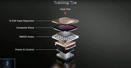
Furthermore, the amount of power consumed would explode moving 8TB/s in and out of such crude packaging. TSMC’s CoWoS has a 3x reticle limit and InFo has a 2x reticle limit. This means Tesla could only package a few chips together. Their only choice was a wafer scale packaging. Specifically, they use a TSMC integrated fan out system on wafer (InFO_SoW).
This is as far as Tesla has gotten. They have an extremely expensive, single tile running in their labs at 2GHz. They do not have a full system. The full system is scheduled for some time in 2022. Knowing Tesla’s timing on Model 3, Model Y, Cyber Truck, Semi, Roadster, and Full Self Driving, we should automatically assume we can pad this timing here.
The two most difficult technological feats have not even been accomplished. This is the tile to tile interconnect and software. Each tile has more external bandwidth than the highest end networking switches. To achieve this, Tesla developed custom interconnects. And by Tesla, I mean their partner who has deep expertise in interconnects. They are custom interconnect for the tile to tile interconnect. This sort of implementation is incredibly expensive compared to standard ethernet.
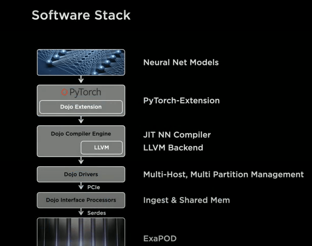
The other lion in the room is software. Tesla does not even claim to have a way to automatically place and route operations of mini-tensors across the architecture. They do claim their compiler takes care of fine-grained and data model parallelism. This handwave here is not enough for us to believe the claim. There are simply far too many firms with AI hardware that can’t even scratch this with many engineers working on the software for chips that have existed for a couple years. Even if they claimed they did, a magical compiler is something worth being skeptical against. When asked questions about the software stack in the Q&A they were woefully unprepared. They even said they had not solved the software problem.
Most likely, the Tesla researchers would need to manually do portions of this process. Furthermore, researchers will need to explicitly address the SRAM or they risk running very quickly. These constraints force their developers to tweak models and optimize them heavily for a system that was supposed to remove the shackles for scaling to massive models.
The biggest question that has been asked by semiconductor professionals has been “How on earth is this economically viable?” Tesla is detailing a very specific set of hardware that isn’t exactly that high volume. Only a total of 3,000 645mm^2 7nm dies have been committed to being deployed. This comes alongside very exotic packaging and custom interconnects developed just to be deployed in the ExaPod supercomputer. There is nowhere near enough volume to amortize the huge costs for researching and developing a chip like this. This applies, even though Tesla isn’t the one doing the R&D on the tile-to-tile interconnect or the 112G SerDes.
The concern about economic viability is a non-concern. The use case of this supercomputer is very clear, train an autonomous driving AI. The end goal and target market are worth trillions. The entire valuation of Tesla is built on the hype that Tesla reaches Robotaxis before anyone else. If they can create and deploy a self-driving AI across the world in millions of cars, then they have justified a trillion-dollar valuation.
To that goal, if this chip and supercomputer system design allow Tesla to reach this target even 6 months earlier, it is worth every penny they spend 10 times over. Many would argue it is debatable they reach it first. There are billions being poured in with very strong competition in this field from the likes of Mobileye, Google’s Waymo, Nvidia and their partners, GM Cruise, Motional, and many others. Of this competition, only Google and Nvidia have supercomputers that stand toe to toe with the Tesla’s. While it is mainly a software problem, an abundance of computing resource helps the researchers iterate faster with more complex neural networks.
Despite the lack of a massive supercomputer, it is widely considered that the Mobileye New York implementation is the most impressive public showcases of autonomous driving. Google’s Waymo has with the fewest interventions per mile driven based on regulatory data. We believe it makes sense for Tesla to pour as much capital as needed into winning the Robotaxi race and catch up to these two. They can very easily raise more capital with cheap debt or further share offerings. Any world where they aren’t the first to a large scale Robotaxi network is one where Tesla is incredibly overvalued. To that end they must pursue this strategy and more.
Elon Musk stated that eventually they could start a SaaS business with this chip/computer. While we don’t know if this will ever be successful, scaling to many of these E1 computers and having that sort of business model would be a big boom.
Cost, custom interconnects, memory constraints, lack of software, and the fact that this chip is 2022 or beyond is something we have to keep in mind. This chip is not Tesla designing something that is better than everyone else all by themselves. We are not at the liberty to reveal the name of their partner(s), but the astute readers will know exactly who we are talking about when we reference the external SerDes and interconnect IP. The Tesla chip and system design is incredibly impressive, but it should not be hyped to the moon.
This article was originally published on SemiAnalysis on August 25th 2021.
Clients and employees of SemiAnalysis may hold positions in companies referenced in this article.


