The Transformation of Veeco
Semiconductor Capital Equipment For EUV Masks, GaN Power and RF, Advanced Packaging, Gate All Around Laser Annealing, MicroLED, And Hard Drives
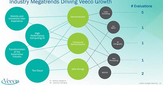
Veeco is relatively small as far as it goes for the space of semiconductor capital equipment. They have also historically undergrown the titans of the industry such as Applied Materials, Lam Research, ASML, Tokyo Electron, and KLA. On a first glance would say you should ignore this company and that they are a relic of the past that continues to lose market share, but their future is far more interesting with a large new facility in San Jose and an array of products serving growing segments. Is Veeco pulling an amazing turn around?
Veeco historically was heavily involved in the worst two businesses for a supplier. Their ion beam deposition and etch tools are critical for hard drives heads and metal organic chemical vapor deposition (MOCVD) for LEDs. The hard drive business is a good business, but it’s quite cyclical. Moreso than even front-end semiconductor equipment. The LED business has been plagued by lower margins due to high competition from China.
In 2017, Veeco acquired Ultratech and in 2018 they exited the commodity LED business. Moving forward their new tools and enhanced capabilities are picking up steam, but is this a successful turnaround in the making?
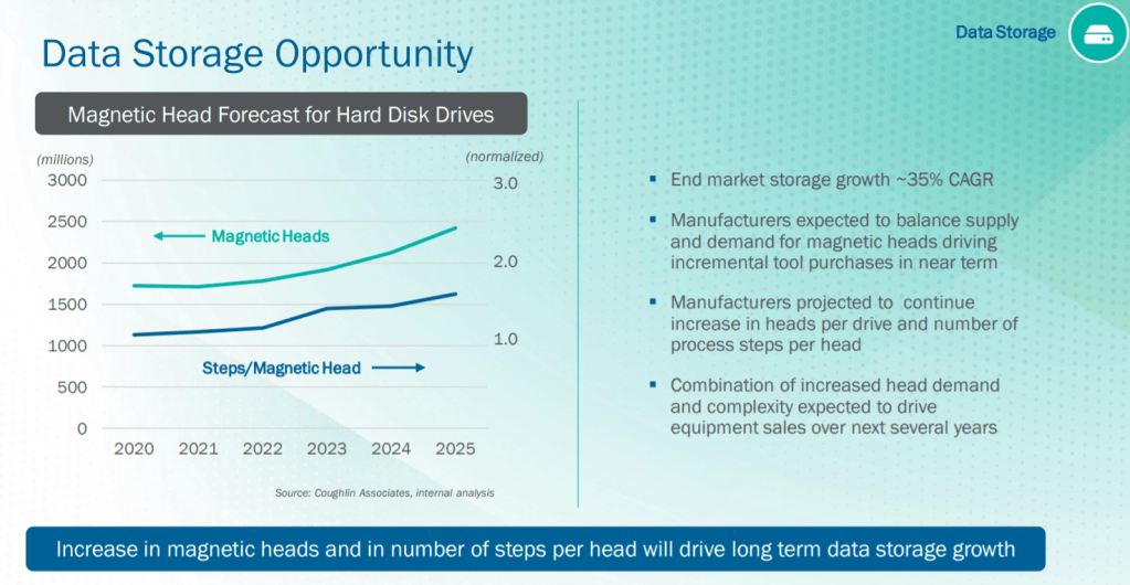
Starting off with some more information on hard drives, they had flatlined for a while as the datacenter boom had still not taken hold and PCs were rapidly ditching hard drives in favor of NAND based SSDs. These dynamics seem to be in the rear-view mirror as the datacenter demand is ferocious. Seagate and Western Digital are quite committed to shipping more and more bits every year.
There are multiple levers where Veeco may be able to ship more tools. One is via more magnetic heads needing to be manufactured and the other is via heads becoming more complicated. As multi actuator hard drives become more common and the typical hard drive contains more platters. There is a magnetic head for every platter and therefore the number of heads expands. Furthermore, as platter density is increased, the complexity of the heads also increases. The hard drive business is still cyclical, but it’s also more clearly a growth market.
Veeco’s other traditional market of MOCVD for LEDs has gone through a tumultuous time. Aixtron is the largest firm operating in the MOCVD, but Veeco outcompeted them in the LED market causing Aixtron to refocus on other MOCVD markets such as lasers, power, and RF. This left Veeco dominating the market for MOCVD related to LEDs. At their height, Veeco had over 50% of their sales coming from China, with most of these being epitaxial tools for the LED market. This success was very short lived as China entered the market.
AMEC, a Chinese semiconductor capital equipment firm entered the field and quickly took share in LED. AMEC would have issues shipping those MOCVD tools outside of China due to IP issues (hint hint). AMEC through a combination of subsidies, low R&D overhead, and selling tools at cost, quickly came to dominate the market. This caused Veeco to exit the market.
During this exit period, they dropped from ~30% of the epi market to 12%. Their main competitor, Aixtron, went from ~30% to ~40% share during the same period. Quite the divergence. Going forward, the MOCVD share losses have stabilized and may even reverse. Veeco regeared their R&D and is tacking the RF, Power, and microLED markets.
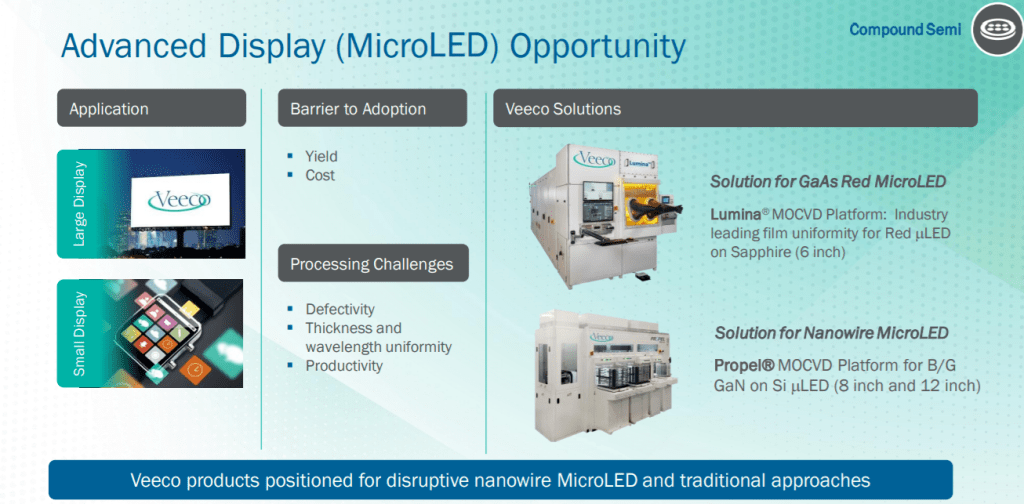
Within the microLED, Veeco serves two markets, one being for red microLEDs that are then pick and placed. This market likely remains small for a long time to come. The Propel nanowire microLED tool could become a big contributor in the future if monolithic microLEDs. Keep track of Aledia, one of their early customers. They are a promising French start up in the space hoping to ramp a new manufacturing process. MicroLED is the holy grail of display technology, it’s just a matter of whether it becomes cost effective to scale.
The much larger opportunity in the short term is the power and RF market. Veeco is the leader in GaN deposition which is heavily utilized in certain RF processes and in power. Aixtron has larger share within this space, particularly because more GaN processes currently are 150mm wafers, but Veeco is better positioned for the future due to their much higher share in 200mm wafer systems. 200mm wafer systems will start to become a much larger portion of GaN on Si and GaN on SiC wafers as new power and RF applications ramp. These tools are also selling the photonics market and have recorded large wins there.
Veeco offers a wet processing system that is doing very well in the RF semi market. They are winning big sales here as well. It is a big driver of their compound semi business unit. This wet processing systems is used for metal lift off and wafer cleaning. The wet processing is also used in the fabrication of HBM memory. For wafer cleaning and metal lift off between DRAM layer stacks. We were able to find out that Micron is a purchaser of their wet processing equipment.
This wet processing HBM win could be because Veeco has a niche within advanced packaging in fan out wafer level packaging and 3D packaging. TSMC, ASE, Samsung, and Intel have purchased lithography tools from Veeco. Veeco is a holds 50%-60% share and this segment is booming. The lithography tool comes from their acquisition of Ultratech. It is used to pattern copper pillars and TSVs. The tool is not as precise as those from Nikon or ASML, but it is higher throughput and therefore it has better TCO. Processes such as Foveros, InFO, CoWoS FoCoS, HBM, FOSiP, and more can utilize this tool. Check out this article for a deep dive on the various advanced packaging types. Veeco’s lithography unit has quite the growth opportunity.
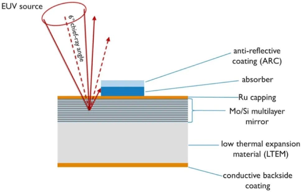
Another very promising growth vector is Veeco’s EUV mask deposition group. Veeco has a complete monopoly on ion deposition tools which sell into this field. EUV masks function very differently from normal masks in that they are reflective. Instead of shining light through a mask and then exposing a wafer, an EUV tool bounces light off a mirror which also happens to be the mask. Join the newsletter, because we will be doing a deep dive on the blueprint of semiconductors, masks, in the next couple weeks.
Veeco’s tools do the molybdenum and silicon deposition as well as the ruthenium capping. Hoya is the majority 80%+ supplier in the EUV mask blank world and Ashhai Glass is also there. Both buy tools from Veeco for these two critical steps. Veeco claims a there is a third recent entrant into this space who is also purchasing tools from them, so if you know who that is, please reach out.
The last product segment that is getting major wins is the laser annealing segment. This segment also comes from the Ultratech acquisition. This is Veeco’s only product that primarily sells into the front end. While some of the segments Veeco sells into are nice niches, the front end is the holy grail for all semicap companies. The laser annealing system is quite an interesting system that is getting wins even at a major logic semiconductor. Veeco claims it is better than a competitors laser annealing system. We believe the competitor which is losing share is Hitachi.
The main benefit with laser annealing is that it is selective. Within a process there is the issue of lowest common denominator and a whole wafer flash annealing step would heat the entire wafer which would cause that lowest common denominator structure to have defects. Laser annealing solves this by only targeting local areas.
Advanced logic nodes require higher temperatures for dopant activation with shorter time at that temperature to avoid dopant diffusion. Annealing the drain in gate all around is another market for Veeco. More information on their big win in this arena for this tool, the financial outlook, and whether or not we like the stock in the subscriber only section.


