TPUv5e: The New Benchmark in Cost-Efficient Inference and Training for <200B Parameter Models
Latency, Performance, Fine-tuning, Scaling, and Networking
During its Cloud Next 2023 event, Google has announced general availability of its latest AI chip, the TPUv5e (TPUv5 lite), and it is a game changer, due to the performance/TCO that it brings for both Google and the new Cloud TPU customers. It is straight up a massive cost advantage for many external parties to train and inference models with less than 200 billion parameters.
TPUv5e also enables Google to inference models that are larger than OpenAI at the same cost as OpenAI’s smaller model. This will massively help Google level the playing field, because they can play the brute force game that no one else can. OpenAI will have to rely on being much smarter with their chips and algorithms due to the massive compute deficit versus Google. AI chips from Amazon (Trainium/Inferentia), Meta (MTIA), and Microsoft (Athena) are all nowhere close to where Google is.
Today we want to detail this game changing chip by demonstrating its performance/TCO advantage with data for cost of training GPT-3 and cost of inference for LLAMA-65B. Furthermore, we want to discuss list price as well as discounted cloud pricing being offered by Google, and how that compares to various GPU pricing.
Hilariously, it makes economic sense for OpenAI to use Google Cloud with the TPUv5e to inference some models, rather than A100 and H100 through Microsoft Azure, despite their favorable deal. Of course, there’s a whole host of political/business reasons this probably never happens.
Before we dive in, we just want to assuage Sam Altman’s concerns. This is in no way Google marketing, and we have no contacts at Google marketing or HR departments. They don’t pay us outside of subscribing to the newsletter. This is analysis based on factual data from Google and a 3rd party AI startup using TPUv5e. The prior he’s referring to are shipments for the full size TPUv5, from supply chain.
To answer Elon, they are not wrong.
Now that we are done being cheeky, let’s discuss the chip and system before moving onto real performance. The TPUv5e (TPUv5 lite) is the successor to the TPUv4i (TPUv4 lite), and should not be confused with the main line of TPUv4 (Pufferfish) and TPUv5 (Viperfish). The TPUv4 lite, which was externally given the i suffix for being an inference chip. The TPUv5 lite, now has the e suffix for efficiency. In the past, most of our focus has been on the full-scale chips, despite the lite chips being used heavily in Google’s internal inference workloads. From TPUv4i to TPUv5e, this changes, because the small chip actually makes sense to use externally.
The TPUv5 and the smaller sibling, TPUv5e, are clearly not designed for peak performance at the cost of everything else. They are both significantly lower power, memory bandwidth, and FLOPS than Nvidia’s H100. This is a conscious decision by Google, and not just an indicator of worse chip design. Google, due to designing and acquiring their own chips through Broadcom, pays significantly lower margins for them. As such, power consumption, networking cost, system cost, and deployment flexibility are much larger indicators of the total cost of ownership (TCO) for the chip over the course of 4+ years.
In Nvidia’s model, due to their massive gross margins on the hardware, has their customers TCO equation dominated by Capex. The Opex costs are relatively much smaller. Therefore, it is more logical for pushing the H100 to 2x the power consumption of a TPUv5 and ~5x that of TPUv5e to squeeze out way more performance. Furthermore, differences in Nvidia’s architecture and SKU lineup make it much more conducive to massive chips. Google’s lack of SKUing and massive tensor units, mean they cannot yield harvest or approach Nvidia’s >90% parametric yield on their AI chips. For these reasons, Google goes for a lower power smaller chip, on not only the TPUv5e, but also the TPUv5. The TPUv5e is ~325mm^2.
Google’s TPUs have either one or two Tensor Cores that operate inside of it. This applied to the TPUv4 and the TPUv4i (lite). The TPUv5e (lite) likewise takes a step back from the unannounced TPU v5 (Viperfish). The TPUv5e only a single Tensor Core, unlike TPU v5 which includes two. Furthermore it is half the HBM stacks and at lower speeds. Lastly, the networking is neutered. Each Tensor Core has 4 Matrix Multiply Units (MXU), a vector unit, and a scalar unit. The MXU is based on 128 x 128 multiply/accumulators in a systolic array. MXUs provide the bulk of the compute power in a Tensor Core. Each MXU can perform 16,000 multiply-accumulate operations per cycle. The TPUv5e has 197 BF16 TFLOPS and 393 Int8 TOPS.
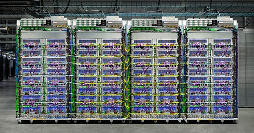
The Tensor Cores communicate with 16 GB of HBM2E memory running at 3200MT/s, for a total memory bandwidth of 819.2GB/s There are up to 256 TPUv5e chips in a pod, there’s which are 4 dual-sided rack unit with 8 TPUv5e sleds per each side. The system had four TPU chips in it, along with a CPU and a 100G NIC. Each 4 TPUs shares 112 vCPUs. These are actually 64C AMD chips, so it appears that Google still requires CPU cores for the hypervisor, and is unable to run it on their NICs.
Google lets you rent up from 1 to 256 TPUv5e with linear cost scaling as you add chips.


Each TPU connects to 4 other TPUs, to the north, south, east, and west at 400Gbps (400G Tx, 400G Rx) via their inter-chip interconnect (ICI). This gives each TPU a staggering 1.6T aggregate bandwidth, which is very high relative to the compute and memory bandwidth of the TPUv5e. Google paid special care to minimizing the number of the number of optics, in a way others don’t, to further reduce the costs. Unlike the TPUv4 and TPUv5, there is no OCS in the ICI inside the pod. The topology is flat. No twisted Torus or anything fancy. This saves a lot on the system level.
Multiple pods can be connected over the Datacenter spine network. The 100G NIC per TPUv5e sled means there is 6.4T pod to pod ethernet based interconnect. In addition, Google has multi-pod available. These inter-pod connections go through the OCS.
Google shared figures for performance scaling all the way up to 4096 TPUv5e’s which is 16 total TPUv5e pods. While that indicates Google has 16 of these pods in 1 datacenter, we believe they have more than 128 TPUv5e pods (32k TPUv5e) in just one datacenter based on the video they released.
As far as software, there is a lot of software Google has made to make this easy to use. This includes everything from compilers to software that makes it easier to batch. While Jax+XLA would work best, the Pytorch+XLA backend is still pretty good performance, meaning many can get away with little to no code changes. For most, to take an existing LLM and run inference, it is as easy as a GPU and perhaps easier to get high utilization than an Nvidia GPU because good GPU inference requires a lot of manual work. This is mostly due to the closed nature of TensorRT making it unusable for anything outside cookie-cutter models or further optimizations with Speculative Decoding and FasterTransformers deprecation/lack of effort.
Below let’s share training costs for a TPUv5e pod vs A100 and H100s for GPT-3. Furthermore, lets also share the inference costs for LLAMA-65B. Inference latency will also be shared.


