Ventana RISC-V CPUs Beating Next Generation Intel Sapphire Rapids! – Overview of 13 RISC-V Companies, CPUs, and Ecosystem
SiFive, Tenstorrent, Rivos, Codasip, Akeana, Alibaba, Imagination, Western Digital, Andes, Krakatoa, MIPS, XMOS, and Ventana
Last week we attended the RISC-V Summit in San Jose. Traction in the RISC-V ecosystem is accelerating faster and faster. The embedded world has shipped 10’s billions of RISC-V cores collectively over the last few years. Qualcomm has silently shifted control and security cores that are not exposed to the user since the 2020 S865 chip. This has enabled them to ship a total of 650 million RISC-V cores! Andes and Codasip are each at over 2 billion RISC-V cores shipped, Western Digital ships over a billion RISC-V cores a year, and even Apple is converting some non-user-facing functions to RISC-V! Google also announced that Android works on RISC-V, and tier 1 vendors will have RISC-V-based phones sooner than most expect.
The soft underbelly of Arm is being attacked extremely quickly by RISC-V cores from SiFive, Codasip, Alibaba, Imagination, Western Digital, Andes, XMOS, and MIPS. RISC-V will surpass Arm in the embedded and micro-controller space by 2024 or 2025. Further on in this report, we will also share some shocking details we learned about Arm’s nuclear option with regard to forced bundling to existing licensees.
The question on everyone’s mind is when RISC-V will come to user-facing applications. The answer is that this may be closer than people expect. There are currently 4 companies working on large RISC-V cores that compete with the biggest and fastest from Intel, AMD, Arm, Apple, etc. These 4 companies are Ventana Micro Systems, Tenstorrent, Rivos, and Akeana. Each of these companies have teams with impressive pedigrees, but that alone doesn’t guarantee success.
This report will include an overview of efforts and/or cores from the 13 companies listed above. We will focus on high-level items such as go-to-market and low-level details related to cores. The overviews of the cores, where we were able to get the data, include the ISA level, pipeline stage count, in-order vs. out-of-order, issue #, privilege mode, SMP/SMT Support, TCM instructions/data, TCM size, I$, D$, L2, L3, and MMU.
Ventana Micro Systems
Ventana may be the most impressive due to the team, go-to-market strategy, and performance. They are also the closest to a commercial product. Ventana says their core is targeting everything from datacenter to automotive to 5G Edge to AI, and even client, but we believe the most advantageous value propositions will be in datacenters, networks, and 5G DU/RU, at least for the first generation.
Ventana’s team has a long and storied history in the industry, including building the first 64-bit Arm core. Much of that team flowed through the progression of Veloce, Applied Micro, Macom, and Ampere Computing. Ventana has raised $108M total, with enough runway to get to their 2nd generation CPU.


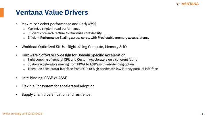
Cutting right to the chase, Ventana’s Veyron VT1 per core performance is comparable to the Neoverse V series from Arm (V1 in Amazon Graviton 3 and V2 in Nvidia Grace) but at higher clocks. Furthermore, it scales up to 128 cores within a 300W power budget. This is comparable performance to what AMD’s Genoa can do. Ventana can also achieve twice the core counts of Amazon’s Graviton 3, albeit with higher power.
Another important distinction is that AMD Genoa and Graviton 3 are measured in silicon and available to customers. Ventana’s performance figures are a simulation with the actual tests coming after tape out in Q1. About new product introductions, we generally believe it’s all talk until the silicon is in the lab. Suppose these 1st party figures are missed by even 20%; Ventana will still smash Intel’s current generation Ice Lake and even Intel’s next-generation Sapphire Rapids, which doesn’t ship in high volume until mid-2023.
Before we go into technical details, we want to highlight the strength of the go-to-market strategy. Ventana isn’t only targeting the crowded bog-standard general-purpose CPU market. Ventana is making CPU chiplets that can be integrated into general-purpose CPU markets and various heterogeneous computing use cases. Furthermore, Ventana does not make the IO Die, but partners with firms on them. This unlocks a very different integration and partnership strategy. IO dies can either be taken off the shelf from existing providers or cheaply developed with mostly licensed IO and NOC IPs.
The customers can focus on their use cases and domain-specific accelerators. These domain-specific accelerators can be integrated directly on the IO die, and/or a chiplet can be developed. This strategy could work very well for the hyperscaler market as that is the exact business model they want.
Companies like Amazon, Microsoft, Google, Meta, Alibaba, Tencent, and Baidu don’t like being at the whims of their suppliers who add more layers of margin stacking. Instead, they want to be in control and vertically integrate more of their offerings.
There is no need for every hyperscaler and ASIC to reinvent the wheel. They can buy and integrate high-performance CPU chiplets at a much lower cost than fully packaged CPUs. Furthermore, when it comes to heterogenous compute and customized designs, the CPU chiplet design allows them to keep power and latency between the accelerators and the CPU minimal.
An IO die can be developed and taped out on TSMC’s 16nm for ~$20M. An IO Die on TSMC 7nm can be designed and taped out for ~$30M. This IO die can scale from a couple of memory controllers and a few PCIe ports to a massive amount of IO and networking. The incremental costs to create a new processor with the exact mix of high-performance CPU and dedicated ASICs integrated into the IO die or as a chiplet is relatively low, given the volumes of hyperscalers.
This business model can extend to the processors for 5G ORAN in the DU and RU, edge AI, edge gateway, in-memory databases, app/web hosting, storage servers, load balancers, caching appliances, content delivery networks, etc. As Moore’s Law crawls and workloads become more targeted by processors, the engineering costs for application-specific accelerators will soar unless an open chiplet approach is taken.


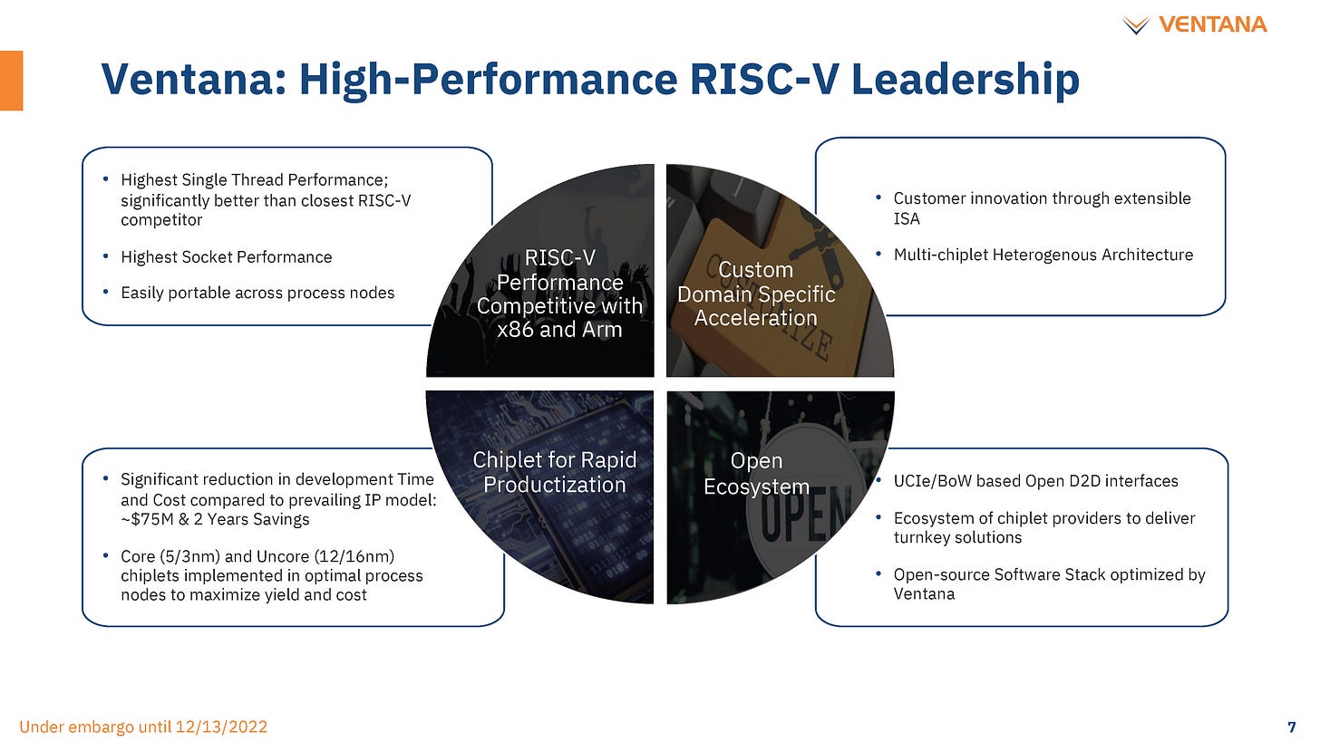
Ventana utilizes the Open Compute Project’s ODSA BOW standard for packaging. We know of at least 4 different compute-type chiplets and at least 3 different IO-related chiplets being made within this standard. While UCIe will be the winner in the long term, in 2023 and 2024, BOW will be more prevalent in the short term. Ventana is planning for future versions to support either BOW or UCIe. The chiplets / IO Die all uses the AMBA CHI protocol, which is much lower latency and power than CXL over UCIe.
While AMD does have a chiplet CPU architecture and a custom silicon business, they do not utilize an open protocol. Furthermore, AMD is not willing to sell only CPU chiplets to hyperscalers. AMD wants to control the vertical stack from silicon design to packaging for any custom silicon deal. This strategy leads to more margin stacking and higher pricing. AMD’s choice makes sense for their business model but also leads to opportunities for hyperscalers to disaggregate them. Intel would follow the same lines as AMD for their business model, but their architecture won’t allow this level of disaggregation until 2025.
Ultimately, Ventana's strongest selling point is bringing the incremental cost of custom silicon to tens of millions of dollars from the current hundreds. When hyperscalers only buy some chiplets from fabless firms and the rest of their silicon directly from the foundries, the incremental cost per deployed package for a specific workload is significantly lower.
The core itself is pretty impressive. It is an 8 wide out-of-order core with a massive 512KB instruction cache. Each core comes with a 3MB L3 cache slice, although this is easily configurable in future versions. The goals with the core are quite simple but tough to achieve. Maximum single-threaded performance, maximum core density, efficient scaling across cores, and predictable/low latency across cores. It is noteworthy that VT1 does not have the RISC-V Vector extensions, as those were ratified too late into the design process. VT2, a relatively fast follow-on, will have the RISC-V Vector extensions.
The chiplet Ventana has developed scales up to 16 cores. One would think a chiplet with 16 big, high-performance CPU cores would result in a large die, but that’s perhaps the most impressive part about Ventana’s solution. The chiplet is 62mm^2 on TSMC’s N5 process technology. Compare that to AMD’s 8-core Zen 4 chiplet on N5, which is larger than Ventana’s 16-core chiplet.
The economics are impressive. Ventana is also designing its CPU to make it easier to port across process nodes. For example, Ventana has a partnership with Intel’s IFS accelerator program, and we believe they will tape VT2 on Intel’s 3 or 18A process technology.
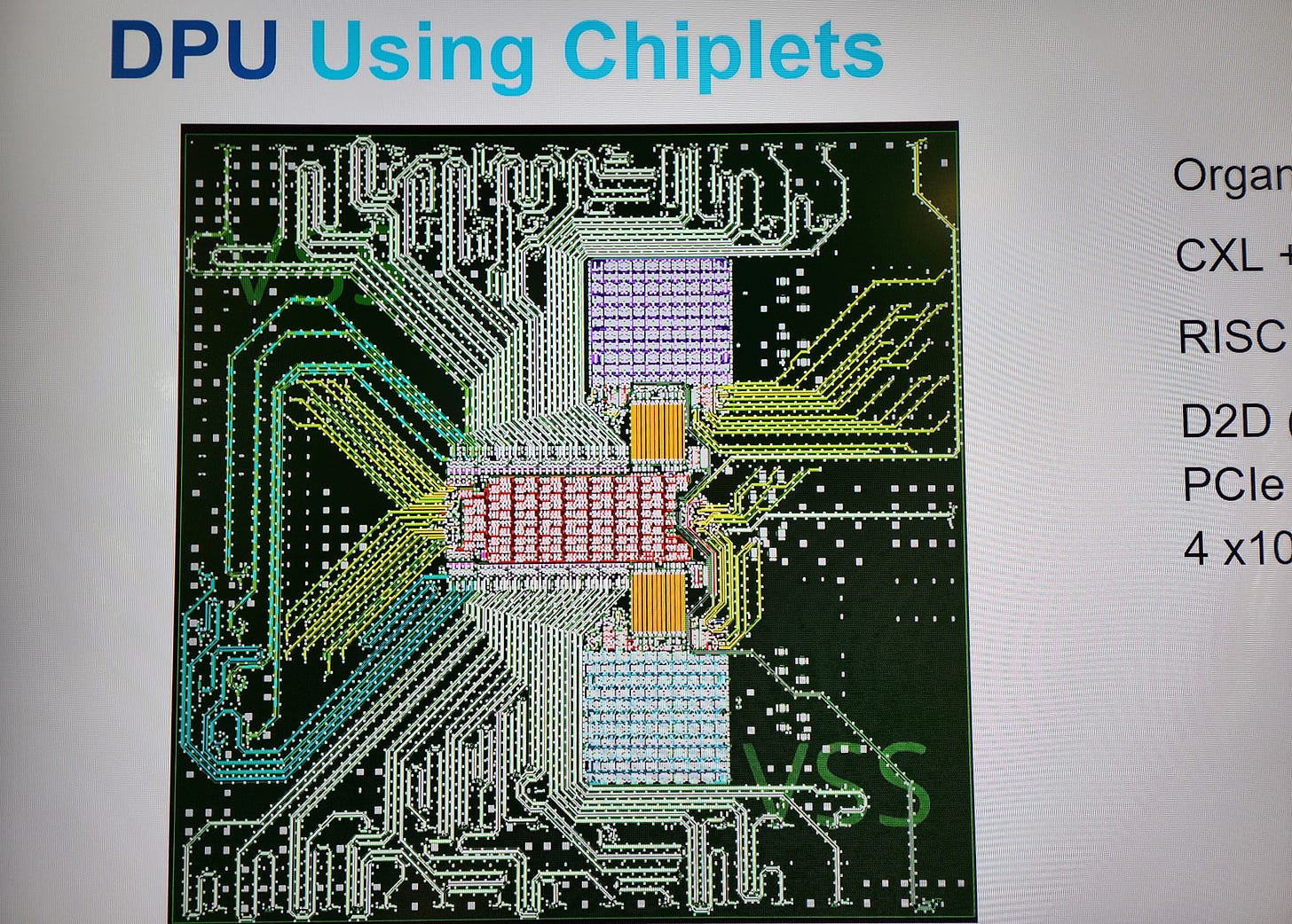
The picture above shows one of the multiple packages designed for Ventana VT1. This specific IO Die contains significant networking capabilities such as ethernet, packet processing, and CXL 2.0 into a DPU. Ventana uses BoW for their chip-to-chip interconnect with this IO Die with 1Tbps in each direction. That link has less than 2ns of latency from the PHY-to-PHY connection with <0.5pj/bit transferred between the IO die and CPU core chiplet.
Compared to Intel’s Sapphire Rapids, this is lower latency (<2ns vs. 2.4ns) and lower power (<0.5pj/bit vs. 0.5pj/bit), and compared to AMD’s Zen 4, this is lower latency and much lower power (<0.5pj/bit vs. <2pj/bit). The Ventana chiplet package is a standard 8-2-8 organic substrate with 130um microbumps, whereas Intel had to use their more costly EMIB advanced packaging with 55um microbumps to achieve those results.
With the right go-to-market strategy and impressive performance, Ventana could be successful, but the software story is also a big part of the conversation. It took Arm a decade from announcing their push into server to getting deployed en mass. RISC-V will take a lot less time because the systems and software are more equipped to switch, but it is a big concern. Ventana knows this just as well as anyone else, where many members of the team experience exactly these teething pains as the first 64-bit Arm core and through their legacy to Ampere Computing.


Ventana claims to have a ton of software for many applications ready, especially on the low-level, storage, and networking applications. Ventana has been able to work on software without its own silicon by using SiFive-based development boards, which have ISA compatibility. In that sense, the challenge of bringing the server software ecosystem to RISC-V started 3 years ago. If Arm took 10 years, and RISC-V is on an accelerated timeline that will take half the time, then potentially, we are only a couple of years away from RISC-V in the datacenter.
That’s the optimistic view, of course. We expect 5G ORAN, networking, and hyperscale internal workloads to be able to jump potentially sooner, but general-purpose multi-tenant cloud instances are much, much further away. The development kit with Ventana’s CPU chiplet will be available in the middle of next year, with volume shipments late next year.
Next, we will compare the leading RISC-V companies. These firms are Ventana, SiFive, Tenstorrent, Rivos, Codasip, Akeana, Alibaba, Imagination, Western Digital, Andes, MIPS, XMOS, and Krakatoa. They are all designing RISC-V cores. Four of these firms are even targeting extremely high-performance cores that compete with AMD and Intel’s server-class cores in single-threaded performance. This includes an overview of their respective strategy and the companies. We will also share some shocking details regarding Arm’s anti-competitive bundling.
At the end of the report, there will also be a table with technical specifications, including ISA level, pipeline stage count, in order vs. OoO, issue #, privilege mode, SMP/SMT Support, TCM instructions/data, TCM size, I$, D$, L2, L3, and MMU.
SiFive
SiFive is the most well-known and successful firm in the RISC-V space. They have already sold a business unit to AlphaWave for $175M. SiFive has a very impressive valuation and a ton of runway. They are going in everything from next-generation TPUs to NASA’s scalable space chiplets. Suffice to say, SiFive has a ton of cores, and X280 is the one we get the most excited about. We will only put the X280, P470, and P670 in the core table below. SiFive’s sea of different CPU cores are regularly updated despite a pretty lean operation. This is due to their use of Chisel.
Chisel is a hardware design language used for designing CPUs. It is a relatively new language whose entire goal is to make it easier for hardware engineers to create complex designs quickly while still allowing them to achieve high performance. Chisel is written in a Scala-like intermediate language to create Verilog-based register-transfer-level (RTL) descriptions of digital circuits. From here, the process is similar to any other chip design flow. The Verilog is synthesized into a lower-level, gate-level description. This gate-level description is then used to create a physical layout of the circuit and create the actual chips.
Many classic CPU architects have issues with Chisel and complain about the lack of performance, difficulty in closing timing, and difficulty debugging. They also state that fixing any of these issues with timing or debugging requires multiple steps of synthesis, going back to the high-level language to fix, and repeating the cycle. We aren’t well versed enough to understand the nuances here; at a high level, the question is whether people should still be designing hardware the same way they were 20 years ago or if there should be some major changes.
The benefits and negatives of a higher-level language vs. a lower-level language play out across software. SiFive is bringing this argument into the limelight within the hardware world.


