Wafer Wars: Deciphering Latest Restrictions On AI And Semiconductor Manufacturing
China's Countermove: How Beijing is Dodging New Semiconductor Restrictions
Last week the US government launched the latest return salvo in the 21st centuries’ cold war. It covered AI chips and wafer fabrication equipment. Today we want to dive into the impacts, what exactly is banned, and what China is doing to work around the new regulations. We will also cover the major remaining gaps in the export controls that China will be able to exploit. Furthermore, we will dive into the impacts to various companies, how we see this playing out in earnings going forward, and China’s retaliation.
AI Semiconductor Controls
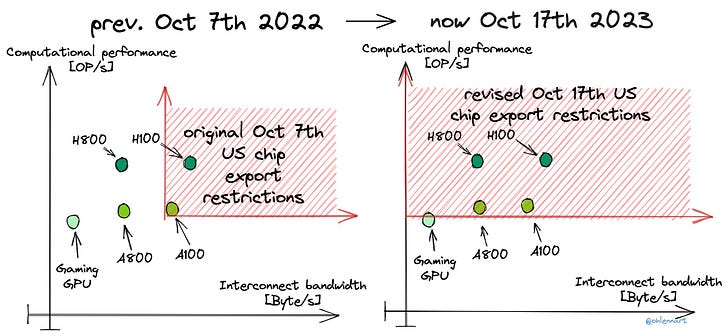
The restrictions around AI semiconductors are very strong and close most of the loopholes. The previous test was aggregate bidirectional transfer rate of 600 GB/s AND aggregate TOPS x bit length of 4800 or more. This meant that companies could easily release new chips with slightly lower aggregate bidirectional bandwidth while maintaining near identical performance in actual AI applications. This is what Nvidia did with the H800 and A800 modifications of their H100 and A100, which have shipped hundreds of thousands of units to China.

Solving this loophole meant the complete removal of the bandwidth limitation, which blocks the A800 and H800. It also means chips such as Intel’s Gaudi 2, Gaudi 3, AMD’s MI250X, and MI300 are all blocked as well. The compute requirement remains broadly the same at TOPS x bit length of 4800, described as “Total Processing Performance” (TPP).
While total chip performance is important to restrict, the government recognized that still leaves multiple loopholes. For example, an AI supercomputer could easily be designed where each chip individually does not breach the performance threshold, but when interconnected together at high bandwidth, it could easily exceed performance thresholds.
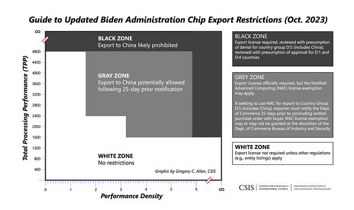
As such, there is also a new performance density threshold too. Performance density is TPP divided by die area. This prevents shipments of chips with smaller die size that have less absolute compute power alone but are still dense/efficient from a computing standpoint. These figures stand at 5.92 for an absolute ban and 3.2 for license. They also come with a few tiered performance levels as well.

This new ruling is incredibly strict. It blocks a variety of GPUs that we believe the market and firms like Nvidia did not expect. This captures chips like the L40S, which was taking advantage of dumb buyers who read topline specs related to TFLOPS and expected it to perform similarly to the A100. Furthermore, many in the Taiwan supply chain expected to be able to ship this chip to China following the long-rumored bans of the A800 and H800. Note our estimates from many months ago on CoWoS, HBM, and Nvidia’s ramp were always expecting a ban in Q4.
Furthermore, the restriction surprisingly blocks the L4, a GPU that is significantly under the bar that even China hawks want restricted. It should be noted that this is due to the GPU’s performance and density. There is a lower bar that would require a license for GPUs such as the 4090, L40, and AMD MI210. Based on our reading, and the lines about being designed for the datacenter, we believe the 4090 will be granted a license.

Furthermore, some viewpoints of the new rules could consider the 320 TFLOPS of FP8 matmul + FP16 accumulate as surpassing the restrictions on even the RTX 4080, and as such also require a license. Given it is not designed for the datacenter, again, we would expect the government to grant a license here.
The question that many people have asked us over the last week is whether Nvidia would be able to go around the bounds of this by making another China specific chip again.
The short answer is, no. Nvidia has no way to really game these rules even with a brand-new clean sheet design. Due to the density rule, they basically have to jump all the way back to the V100, which was released in 2017 and based on 12nm. Nvidia can’t stuff a bunch of blank silicon to get around the density rules because the regulation accounts for that. It fundamentally bans all high-performance ASICs that people are currently developing, which means large transformers simply cannot be run efficiently on any hardware that passes the regulations.
Currently, the industry overfits to exploring AI techniques that work well on existing chips, i.e Nvidia GPUs/Google TPUs running variants of transformers. With the AI Accelerator sanctions on China, one interesting result might be that China forks silicon and explores a different idea-space in AI techniques than the rest of the world. After all, the brain and the signals propagating on it look nothing like our current hardware/software architectures either.

China will invest heavily in compute in memory, neuromorphic computing, or some other analog approach. Currently, none of these approaches show promise in transformers or diffusion models, but that says nothing of new model architectures.
The short-term path forward is with Huawei. Huawei has taped out a 7nm ASIC on SMIC’s N+2 process node. It is a successor to the Ascend 910 that Huawei launched back in 2019. We hear this chip utilizes chiplets and contains HBM. China stockpiled millions of units of HBM from SK Hynix and Samsung this year. It is not clear where these are being deployed, because there are no high-volume chips domestically produced in China that can utilize these HBM stacks. The only logical conclusion is that these were imported for Huawei’s upcoming chip.
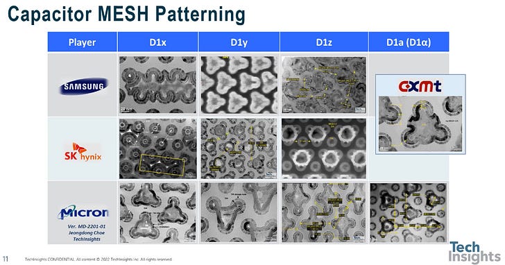
Hawuei’s Ascend 910 from 2019 already breaks the current regulations, so a domestically produced successor would also beat anything Nvidia can legally ship into the country. While some would argue SMIC is not capable, the fact is that their old 14nm was already used to make an exascale supercomputer. The new N+2 node (7nm) is approaching 20,000 WPM of capacity, which is enough for millions of accelerators at even 50% yields. Furthermore, China is rapidly approaching capabilities of manufacturing HBM domestically at CXMT, but more on that in a bit.
Wafer Fabrication Equipment Controls
We believe the changes to the control list for equipment are much less impactful than those for AI chips. While many areas were tightened, there are still some holes, which enable the various equipment companies such as Applied Materials, Lam Research, Tokyo Electron, Kokusai Electric, KLA, Onto, Screen, ASML, etc to continue to ship tens of billions of dollars of tools to China. This includes over $7 billion of equipment for DRAM fabrication that is slated to go to CXMT, more than US headquartered Micron will spend on the same technology. CXMT is also clearly building what the US considers restricted technologies, yet blind eyes are being turned.

Most of what was added harmonizes with the Japanese and Dutch restrictions. For a quick rundown, this covers tools such as epi equipment for SiGe, certain dry etch equipment for 3d structures, wet etch for SiGe and 3D structures, various deposition equipment related to interconnects, cobalt deposition, certain tools for carbon hard masks, certain Atomic Layer Deposition (ALD) equipment for barriers, liners, and tungsten interconnects, deposition tools related to molybdenum, mask making tools, EUV pellicles, and certain DUV lithography tools.
One puzzling aspect of the 2022 rules was the very limited scope of etch tools that were put under export controls. Under the old regulations only anisotropic dry etch was included. Anisotropic means an etch that is only performed in a single direction (sideways), and dry etch means using a plasma-based etchant to remove material. Now the new regulations expands coverage of etching to isotropic etching as well (vertical).
For wet etch, only wet etch tools that have “SiGe to Si etch selectivity ratio of at least 100:1” is added. Specifically, the process that would be targeted is the removal of the sacrificial SiGe layers used to form the nanosheets for GAA transistors.

The biggest addition is of course the changes to DUV lithography restrictions. BIS added a “dedicated chuck overlay” criteria, following the lead of Dutch export controls, which currently restrict tools with an overlay of below 1.5nm. Overlay in lithography refers to the alignment accuracy between different layers or patterns that are sequentially printed onto a wafer. Good overlay is required for multi-patterning, which is how TSMC and Intel achieved 7nm. The Dutch restriction prevents the shipment of tools such as the 2000i and beyond.
However, the new US rules now go one step further and restrict tools with an overlay of 2.4nm and below, which includes ASML’s 1980i, the tool used for TSMC, Intel, and SMIC’s 7nm technologies. The US is able to restrict these tools with chuck overlay of between 1.5nm and 2.4nm by applying a 0% de minimis threshold, i.e if any part of the tool includes US technology, the tool is subject to license requirements.
Normally the rule for US content is 25%, but in this case, it just has to have any US content. Even if ASML tried, it would take many years to able to redesign their 1980i lithography tools to stop using US technologies related to overlay, OPC, and the light source.
This rule only applies if the tool is used for “development” or “production” of “advanced-node integrated circuits”.
But Only For “Advanced” Fabs
The 1980i restrictions only target “Advanced” fabs which is a bit of a loophole as most fabs will not be classified as advanced. A fab can be built under the pretense it is mature, then turn around and become an “advanced fab”, for example with CXMT.
Due to the loophole, this means that ASML’s newest TWINSCAN NXT:1980Di and Fi series of immersion tools can still be shipped to mature node customers. Furthermore, firms like SMIC can continue to receive these tools at all fabs besides SN1 and SN2, where their 7nm is being fabricated. We believe this is much too lenient, as motivated players can certainly transfer tools. China should be able to service all of these tools domestically within the next 2 years as well.
Beyond the “advanced” fabs loophole, some of the most critical technologies such as hybrid bonding, copackaged optics, TSV formation, and DRAM manufacturing are still left wide open.
Rule Harmonization
Many of the new rules that are implemented to match the last round of Dutch and Japanese export controls. This makes US export controls consistent with them, but also widens the scope of coverage to US companies and/or products that meet de minimis content requirements. The Dutch rules from June placed export controls on lithography tools with overlay below 1.5nm and MRF, US rules now go one step further to overlay up to 2.4nm as we mentioned above. Dutch rules also placed controls on other production equipment supplied by Dutch companies: EUV pellicles and pellicle making equipment (also from ASML); Si or SiGe epitaxy tools, and ALD tools for work function metals (both from ASMI).
The Japanese controls that were introduced in May placed controls on tools relating to Japanese equipment providers: EUV resist coaters/developers (TEL), EUV mask inspection (TEL), dry etchers and wet etch for SiGe (TEL), deposition tools (TEL and Kokusai), epitaxy (TEL), cleaning tools (TEL and Screen) lithography tools (Nikon and Canon). In general, the new US restrictions have been updated to harmonize with the Japanese rules (we note that sometimes the US rules are even word for word copies of translations of the Japanese rules!)
What do equipment companies have to say about these restrictions?
In ASML’s October 18th earnings call, held just a day after the release of the new rules, management acknowledged that the new export controls would effectively restrict equipment sold to China worth about 10 – 15% of the company’s expected total shipments to China on a whole year basis.
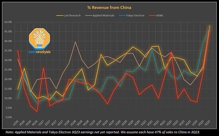
Note that ASML had 46% of their revenue come from China in the most recent quarter, due to a huge influx of rush orders before the long since rumored banned. This means only 5% to 7% of their total revenue in this rush order quarter would have been blocked under the new rules.

Though the company confirmed that the rules in principle ban the TWINSCAN NXT:1980Di DUV lithography system from export to China. ASML characterized this as only impacting “a handful of fabs” due to the “advanced” fabs loophole. Note there are already more than 100 fabs build or under construction in China.
Even ignoring the leading edge, the majority of shipments into China are for the massively subsidized mature nodes. China is going for their tried and true practice of subsidizing, banning foreign competitors domestically, then dumping internationally to gain share from companies like Texas Instruments, STMicroelectronics, Analog Devices, Microchip, Infineon, Onsemi, and NXP. These firms will be kicked out of the Chinese market over the next handful of years, and eventually, some subsegments that are controlled by Chinese ODMs internationally.
Company executives explained that the vast majority of DUV system shipments were to support trailing edge and mature nodes as opposed to advanced processes, driven mainly by electric vehicle, communications, industrial IOT and renewable energy end use cases as well as an overall strategy of reducing reliance on imported chips. They characterized demand from China as highly sustainable because of goal of achieving a level of self-sufficiency – and its current distance from that goal and explained that neither 2023 or 2024 would see a peak in demand from China:
So there is a lot of semiconductor need, and this is exactly when we look at the expansion plans of our Chinese customers. It's exactly what they -- where they are putting their capacity at work in these areas. And if you look at the total consumption of semiconductors by the Chinese manufacturing industry, then China imports more semiconductors than they import oil. On top of that, you see the significant increase in these new transitions. That means that if China wants to come to a certain level of self-sufficiency, yeah, have still a huge gap to cover to be completely self-sufficient. So it's also logical that they actually invest in this type of semiconductor technology because it's for internal use. And I think so it's -- I don't think we will see a peak this year and next year, but I think there will be going forward a significant demand coming out of China for mid-critical and mature technology, and for all the reasons that I just mentioned.
Peter Wennink, CEO of ASML
As for the surge in deliveries to China in 2023, this was explained as being due to ASML seizing the opportunity to fulfil orders for Chinese customers given the push back in demand from other customers, with such surge in demand again for use in trailing edge and mature processes as opposed to any concerted effort by China based clients to beat future equipment bans. Convenient to say the least.
Lam Research – Steady As She Goes
The story is similar at Lam Research, the largest etch company. Their revenue soared 102% quarter on quarter from China to $1,671M, primarily off the backs of rush orders before any potential bans. Management went to great lengths to assure investors of the sustainability of revenue from China:
I don't know if China is up now on our sideways next tier, but it's not going away. When we talk to our customers in China, they all communicate roadmaps that have multiyear horizons in front of them. Nothing new came from the regulations that you saw yesterday. So I see a level of sustainability in China as we go into next year and frankly, beyond. They have long-term objectives.
Doug Bettinger, CFO of Lam Research
A key theme driving these long-term plans is highlighted regionalization leading to sustained demand for investment in mature nodes from China for the next several years.
When it comes to the impact of the rule changes in the October 2023 restrictions, Lam Research does not expect any material impact to the business in part because significant restrictions already apply to some of Lam’s equipment sales to China. Lam Research is the biggest player in 3D NAND, and looks to maintain that for the next few years.
Lam Research was heavily impacted by last year’s sanctions placed on YMTC, China’s state sponsored 3D NAND firm. For some reason, similar actions are not being taken on SMIC, China’s state sponsored foundry, or CXMT, China’s state sponsored DRAM firm, despite both those technologies being far more critical for AI and high-performance computing than flash storage.
The executives at Lam Research also downplayed the possibility of tools purchased for mature nodes being used for advanced nodes, arguing that there are very strict guidelines Lam follows in order to comply with this regulation, and as a result that the prevalence of this customer behavior was probably much lower than feared.
The 9% QoQ rebound in Lam’s Sep-2023 quarter revenue was driven partly by better-than-expected DRAM spending, in particular from the domestic Chinese customer (CXMT). Lam Research specifically said China DRAM offset weakness in DRAM spend for non-China players. The 102% QoQ jump in revenue from China to $1,671M (up 9% YoY, and surpassing the prior high watermark of $1,608M in Sep-21Q) was explained to be driven by domestic Chinese customers as part of the regionalization initiative.
Lam’s management expects sales to China to remain strong into the Dec-2023 quarter and guided for it remain at a similar % of revenue, with total revenue guided to grow 6% QoQ at the midpoint to reach $3,700M.
Long story short, China continues to grow despite the sanctions for Lam Research.
“Is This Time Different?”
Another common thread between both management calls is the in the same breath that management repeatedly point out that the semiconductor industry was highly cyclical and declined to predict timing for industry recovery, they are saying that China investment can only go up and appear to state with confidence that their China businesses will remain strong and sustainable for years to come. In other words, when it comes to China, they are telling investors that “This Time is Different”.
Looking at revenue trends for four major SemiCap companies in the past seven years, combined sales to China have grown from about $1.2B per quarter on average in 2016 (17% of total revenue) to a high of $5.1B per quarter on average in last upcycle in 2021 (28% of total revenue). This is in line with well understood structural growth in semiconductor demand as well as a concerted effort to grow domestically owned production capacity.
The upcycle into 2023 so far, however, has been something else entirely – from a low of $3.7B in 1Q23, combined sales to China have surged to $5.1B in 2Q23, not far off from the prior high watermark of $5.8B seen in 2Q21. Assuming that Applied Materials and Tokyo Electron (which have yet to report earnings for calendar 3Q23) have a similar proportion of sales to China in 3Q23 as did Lam Research and ASML (at 48% and 46% respectively), combined sales to China would reach $8.7B in 3Q23, 50% higher than the prior high watermark from 2Q21.

End product markets tend to be global and interrelated, so it makes sense that the SemiCap investment cycle within China and outside of China has largely been in sync.
We are nearly two years into the current semiconductor downturn (excluding AI-related chips of course) and while industry participants may feel that a rebound should be imminent, there hasn’t been any sharp uptick in actual investment so far, especially ex-China.

That is – except for China, where SemiCap investment has rebounded dramatically and well ahead of the rest of the world. Granted, local auto manufacturers and manufacturing in general in China is shifting away from using western suppliers of mature node and analog semiconductors and is spending 30 years of capex in just a few to achieve that goal, but it seems possible that the near doubling of capex in just a few quarters is also due to something else.

Next we will share a bit about China’s retaliation. This restriction on AI chips and manufacturing equipment is not going untouched.


