Zen 4c: AMD’s Response to Hyperscale ARM & Intel Atom
Bergamo Volumes, ASP, Performance, Hyperscale Order Shift, Die Shot, Floorplan, Physical Design, and Future Use of Dense Core Variants
Bergamo, AMD’s upcoming 128-core server part sets new heights in x86 CPU performance. Architected to be cloud native, Bergamo represents an important inflection point in datacenter CPU design as Moore’s Law grinds to a crawl. At the heart of Bergamo is Zen 4c, a brand-new CPU core variant of their successful 5nm Zen 4 microarchitecture that enables the push toward more cores per socket. While official details of Zen 4c have been rather scant so far, AMD’s Chief Technical Officer had this to say at their Ryzen 7000 Keynote:
Our Zen 4c, it's our compact density that's an addition, it's a new swimlane to our cores roadmap, and it delivers the identical functionality of Zen 4 at about half of the core area.
Mark Papermaster, AMD CTO
In this deep dive, we will share out analysis on Zen 4c architecture, market impact, ASP, volumes, order switches from hyperscalers, and how AMD is able to halve core area while keeping the same core functionality and performance. We will examine why AMD is pursuing this new path in CPU design in their response to market demands and the competition from ARM-based chips from Amazon, Google, Microsoft, Alibaba, Ampere Computing, as well as Intel’s x86 Atom E-cores.
Finally, we look at Bergamo’s reduced production costs and expected sales volumes, and the adoption of dense-core variants across AMD’s line-up in client, embedded, and datacenter going forward. Before diving into those market and architecture details, let’s first share higher-level background.
The Cloud CPU Era at the End of Moore’s Law
The rationale behind the design of Zen 4c and Bergamo is about delivering as many compute resources as possible while battling against the physical limits of silicon as Moore’s Law slows. The slowdown is an industry-wide phenomenon that challenges designers despite demands to continue to increase core counts. As AMD brings their 128-core Bergamo to market, rival Intel is preparing their 144-core “Sierra Forest” part. Both are responding to the rise of ARM CPU cores in the datacenter, from the hyperscaler in-house efforts of Amazon, Google, Microsoft, and Alibaba to the merchant silicon 192-core AmpereOne Cloud Native CPU.
While GPUs, accelerators and ASICs are all the rage with increasing share of capex dollars with the rise of Generative AI, the humble general-purpose CPU still makes the foundational backbone of most datacenter deployments around the world. In the cloud computing paradigm, maximizing compute resources while minimizing Total Cost of Ownership (TCO) is the name of the game.
Increasing core counts is one of the primary ways to save power and cost. Socket consolidation, where a single new CPU replaces four or more old CPUs, is all the rage. There are large fleets of 22 to 28-core Intel CPUs on 14nm that guzzle power and need to be replaced. We have not had an infrastructure replacement cycle since the mid-2010s, and the clouds have extended server lifetimes from 3 years to 6. That is changing soon as the performance/TCO improvements of new Cloud Native CPUs spurs development.
By consolidating, there is less need for slow and power-hungry inter-socket and network communications, and fewer physical resources are required (fans, power supplies, circuit boards etc.). Even in the same generation, two 32-core servers will fundamentally pull more power than one 64-core server offering the same performance level. In the cloud, it is simpler to spin up, wind down, and migrate clients across the compute network with fewer, larger compute nodes.
However, more cores mean more power. CPU socket Thermal Design Power (TDP) have skyrocketed in the last 7 years, from 140W to 400W. 2024 platforms will crack 500W! Despite this, the limits on power and cooling from increased thermal density mean that TDP is not growing commensurately with core count increases, resulting in the power budget per core falling. Running at high clock speeds and power maximizes performance per core and performance per mm² of silicon, the fundamental units of cost.
The trend is that performance per Watt in any given workload is the most important factor, and as such can command a significant price premium. Look no further than the AMD Milan to Genoa transition, where AMD was able to command an 80% price increase simply due to the increased deployment density and performance per watt.
Consequently, CPU architects must be careful in balancing their core designs to optimize for performance per Watt. At the same time, cost per transistor is flat-lining with new process nodes as Moore’s Law slows, so the task gets more difficult as transistor budgets and core sizes needs to be kept in check.
The fundamental design decisions that engineers make multi-variable trade-offs with imperfect information around the performance, power consumption, area, and more. On one end of the Performance, Power, Area (PPA) curve is IBM’s Telum, focusing on maximum performance per core for legacy mainframe-style applications. To improve the product for their banking, airline, and governmental customers, IBM must engineer gigantic cores, 5GHz+ clock speeds, and ultimate reliability that are too costly for newer containerized distributed workloads.
On the other end are CPUs in microcontrollers and low-power mobile chips that prioritize power efficiency and minimum area (cost). Intel’s failure in the smartphone revolution meant they lack the decade of design experience ARM had in power efficiency optimization. The differing design points showed when Apple scaled up its architecture with M1 Macs and blew Intel out of the water. Intel’s high-performance P-core have been getting more and more bloated over the years as they continue to chase per-core performance and 6GHz clock speeds at the expense of power and area. Running that same core under 3GHz in a server chip is not the most optimal for area efficiency.
Intel’s Sierra Forest next year will address this by bringing their E-core design to the datacenter. Spawned from their Atom line of low-power cores, Intel can pack 3-4x the cores for a given die size. However, the caveat with E-cores is their reduced Instruction Set Architecture (ISA) feature level and lower Instructions Per Clock (IPC), leading to worse per-core performance and efficiency. The latter is more than made up for by the sheer core count increase in many workloads.
Intel started combining E-cores with P-cores in their client lineup to boost multi-threaded performance per mm², with the ISA mismatch causing some quirks like disabling AVX-512 on the P-cores and requiring a hardware thread scheduler to manage workload assignment to cores with vastly different characteristics. As for the fully E-core Sierra Forest, its focus is to deliver socket performance close to the P-core Granite Rapids while using far less silicon. Its successor, Clearwater Forest, will then go all out on performance and cores per socket.
Back to AMD, who has neither the smartphone experience nor a separate design team with low power core lineage. Their Zen core must also scale from 5.7GHz desktops to high-efficiency laptops and servers. As a response to ARM and Atom, they created Zen 4c. Zen 4c is a concerted effort by AMD’s design teams to come up with a core that sits on a different point in the Performance, Power, Area (PPA) curve to better suit recent trends in datacenter CPU workloads. In a rather resourceful move, AMD has taken the same Zen 4 architecture and pulled several tricks in physical design to save a huge amount of area.
This means an identical IPC and ISA feature level, which simplifies integration on the client side. In fact, AMD’s is also silently swapping some Zen 4 cores with Zen 4c cores in its lower-end 4nm Ryzen 7000U “Phoenix” mobile processors. On Bergamo, Zen 4c allows AMD to increase core counts from 96 to 128 while saving on area and cost. This bifurcation in design philosophy will increase in future generations of hardware.
Next let’s cover the nitty gritty technical details before finally zooming out and covering costs, ASPs, hyperscaler order switching, volumes, and adoption in non-datacenter environments.
AMD EPYC 9004 “Bergamo” Specifications
Here is the spec table for Bergamo and its differences to Genoa. Two Models will be launching in June: The fully enabled 128-core EPYC 9754 and the cut down 112-core EPYC 9734, with 1/8th of the Zen 4c cores disabled. Comparing to Genoa’s best 96-core EPYC 9654, Zen 4c enables Bergamo to fit 1.33x the number of cores in the same SP5 socket and 360W TDP. Zen 4c has the same amount of private cache as Zen 4, with identical L1 and 1MB L2. Keeping a sufficiently large private cache is important in cloud and virtualized environments. This helps to maintain performance consistency by reducing dependence on shared resources and the impact of ‘noisy neighbors’.
Clock speeds have also dropped with Bergamo, with a 150MHz lower base clock and a 600MHz lower boost clock. Naturally, more cores in the same 360W socket TDP means a lower operating frequency. Bergamo still has a 1.25x advantage in raw CPU throughput (cores x base clocks), and while Genoa can boost higher, that only helps in lower utilization scenarios. Bergamo focuses on cloud environments where predictable performance is key, with a lower working range of clock speeds.
The other major difference with Bergamo is in the die and L3 cache configuration. The number of CCDs drops from 12 on Genoa to 8 on Bergamo, meaning each CCD has 16 Zen 4c cores on Bergamo compared to 8 Zen 4 cores on Genoa. Bergamo also sees the return of multiple CCX per CCD, last seen on the EPYC 7002 “Rome” generation. This splits the die in two, where cores on one half can only communicate to the other half by making a long round trip across the IO Die.
The performance implications of this will be detailed below. While Bergamo still has 8 cores per CCX that can communicate locally, their shared L3 cache has been halved to 16MB. This half-size L3 is also seen on AMD’s mobile designs in a bid to save area. While this will hurt IPC in some workloads, this makes sense for Bergamo, with less focus on shared resources and more on performance per mm². Those looking for a large L3 option can look forward to Genoa-X with its whopping 1152MB of L3.
Bergamo uses the same IO Die as Genoa, so the SP5 socket IO is identical with 12 channels of DDR5-4800, 128 PCIe 5.0 lanes, and dual-socket capability. However, Bergamo’s IO Die only connects to 8 CCDs vs 12 on Genoa, which brings the question: Could AMD have done a 12 CCD, 192-core Bergamo? Other than a much lower power budget and memory bandwidth per core, the silicon could theoretically support it. However, the package cannot.
The IO die has 12 Global Memory Interconnect 3 (GMI3) chiplet links, routed through the package substrate. In Genoa, the GMI3 wires for CCDs farther away from the IO Die are routed underneath the L3 cache area of the nearer CCDs. As it turns out, this is more difficult on Bergamo, as the Zen 4c CCD’s higher density means the wires must be routed under the smaller L3 of the nearer CCD using more layers. We can see the visual result of this with the CCD die placement. On Genoa, there are groups of 3 CCDs placed right beside each other, while there is a gap between CCDs on Bergamo to make space for routing. The package also routes PCIe through the middle and DDR5 above and below, so the available space is insufficient for 12 Zen 4c CCDs.
Die shot, Floorplan, and Core Analysis
Here is the dieshot of Bergamo’s Zen 4c CCD, codename “Vindhya”. This was made with assets from the Zen 4 CCD, codename “Durango”, provided by AMD at ISSCC 2023. Notice the two 8-core CCX Compute Complexes beside each other, each with 16MB of shared L3. The L3 also lacks the arrays of Through-Silicon Vias (TSV) for 3D V-Cache, giving a small area saving. This makes sense as cloud workloads do not stand to benefit as much from large amounts of shared cache.
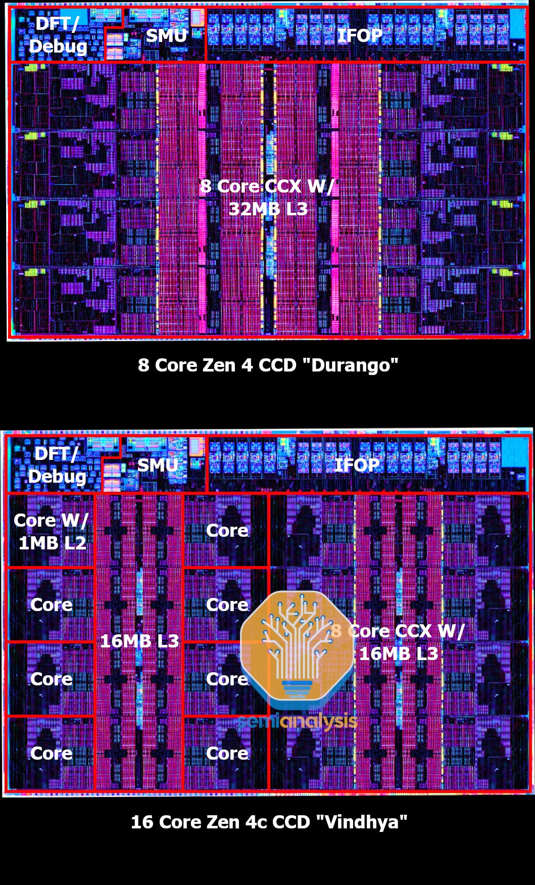
However, the truly stunning thing here is the die size. 16 Zen 4c cores are barely larger than 8 Zen 4 cores. At ISSCC 2023, AMD disclosed Zen 4’s CCD to be 66.3mm². This is the design area without die seal and scribe lines at the edges. Zen 4c’s CCD design area is just 72.7mm², not even 10% bigger! Keep in mind that there are double the cores, double the L2 cache, and the same amount of L3 cache on each die. The cores must have shrunk greatly to fit even more cache per die with only a small area increase.
With regards to the chiplet interconnect, the Infinity Fabric on Package (IFOP) is the same on both dies, comprising two GMI3-Narrow links. However, while the die supports it, there does not appear to be a Zen 4c model that uses both GMI3 links. Instead, signals from the two independent CCX are muxed through a single link to the IO Die.
A closer look at the cores reveals the stark difference in design and layout. Here is a table with an area breakdown of Zen 4c, codename “Dionysus”, compared to Zen 4, codename “Persephone”.
Core Area dropped by 35.4% for Zen 4c vs Zen4, which is remarkable as it is inclusive of the 1MB L2 cache on each. While this means the L2 SRAM Cells take up the same area, AMD were able to reduce the area of the L2 Region by making the L2 control logic more compact. Excluding the L2 and Chip Pervasive Logic (CPL) Regions, the core shrank by an incredible 44.1%, with the engine (Front End + Execution) area nearly being cut in half.
This is what Papermaster is referring to, an amazing feat of engineering as Zen 4c is fundamentally the same design as Zen 4 with the same IPC, just implemented and laid out differently. The Floating Point Unit (FPU) did not shrink to quite the same degree, likely due to thermal hotspots, as the FPU is usually the hottest part of the core when heavily stressed. We also note that the SRAM Cells within the core itself also seem much more compact, with a 32.6% area reduction. You can see this clearly with the Page Table Walker on the bottom right.
Physical Design Tricks
AMD created Zen 4c by taking the exact same Zen 4 Register-Transfer Level (RTL) description, which describes the logical design of the Zen 4 core IP, and implementing it with a far more compact physical design. The design rules are the same as both are on TSMC N5, yet the area difference is massive. We detail the three key techniques of device Physical Design that enables this.
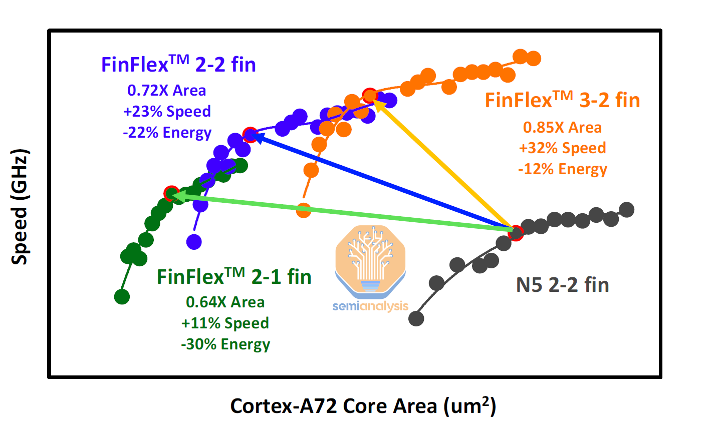
First, lowering the clock target of a design can lead to reduced area when the core is synthesized. Here is a Speed vs Area curve for an ARM Cortex-A72 CPU Core synthesized on TSMC’s N5 and N3E nodes. Even with the same core design on the same node, there is a choice with the area of the core and the clock speed achievable on it. With a lower clock target, designers have more working room with the design of critical paths, simplifying timing closure and reducing the number of additional buffer cells required to clear relaxed timing constraints. With most designs nowadays being limited by routing density and congestion, a lower operating clock enables designers to squeeze signal paths closer together and improve standard cell density.
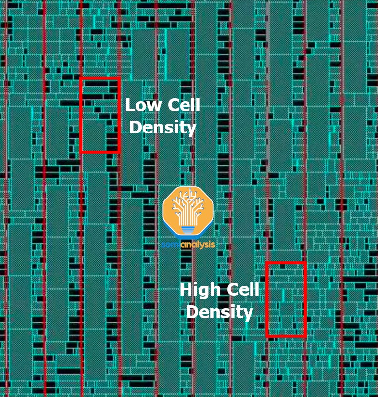
Standard cell density refers to the proportion of placeable area in a design that is occupied by standard cells. Standard cells are functional circuits such as Flip Flops and inverters that are repeated throughout a design and combined to form complex digital logic. These come in many different sizes as seen in this closeup view from placement software. Blue rectangles are the standard cells, while the black regions are unfilled. We have highlighted a region with low cell density, about 50% area utilization, and another with high cell density, above 90%. Standard cells with a high number of input and output signal pins can strain wire routing resources nearby, effectively blocking the adjacent space for standard cell placement.
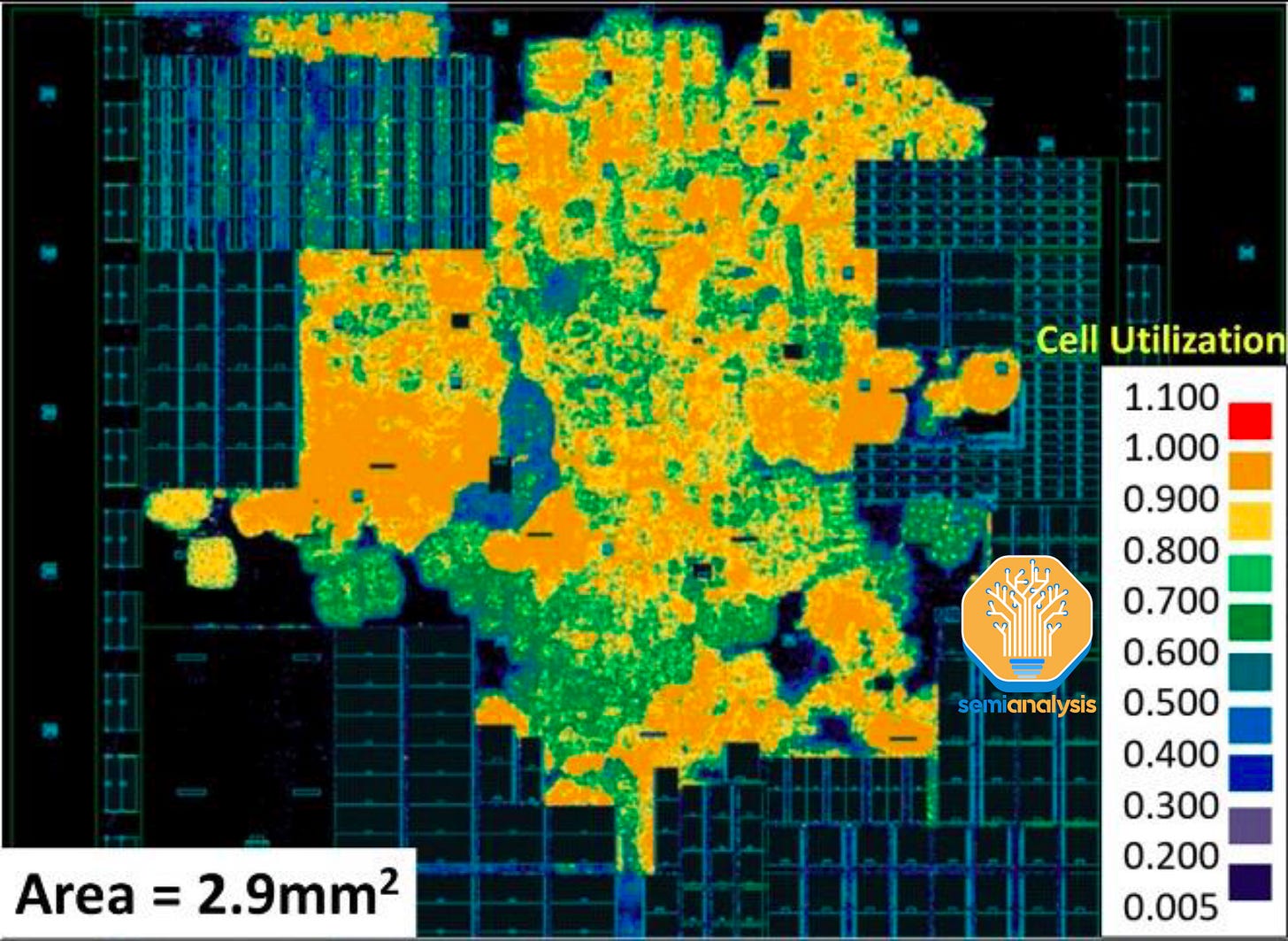
Zooming out to view the core as a whole, a cell density plot can be generated that gives an overview of regions where standard cells are tightly packed (orange, yellow), and regions with lower area utilization (green, blue). The black rectangles are large SRAM macros that are positioned before the standard cells are placed. What all this means is AMD could have taken their Zen 4 core and done a direct shrink by moving down the Speed vs Area curve, and the core would look largely similar but with higher cell density. However, Zen 4c looks very different due to the next Physical Design approach.
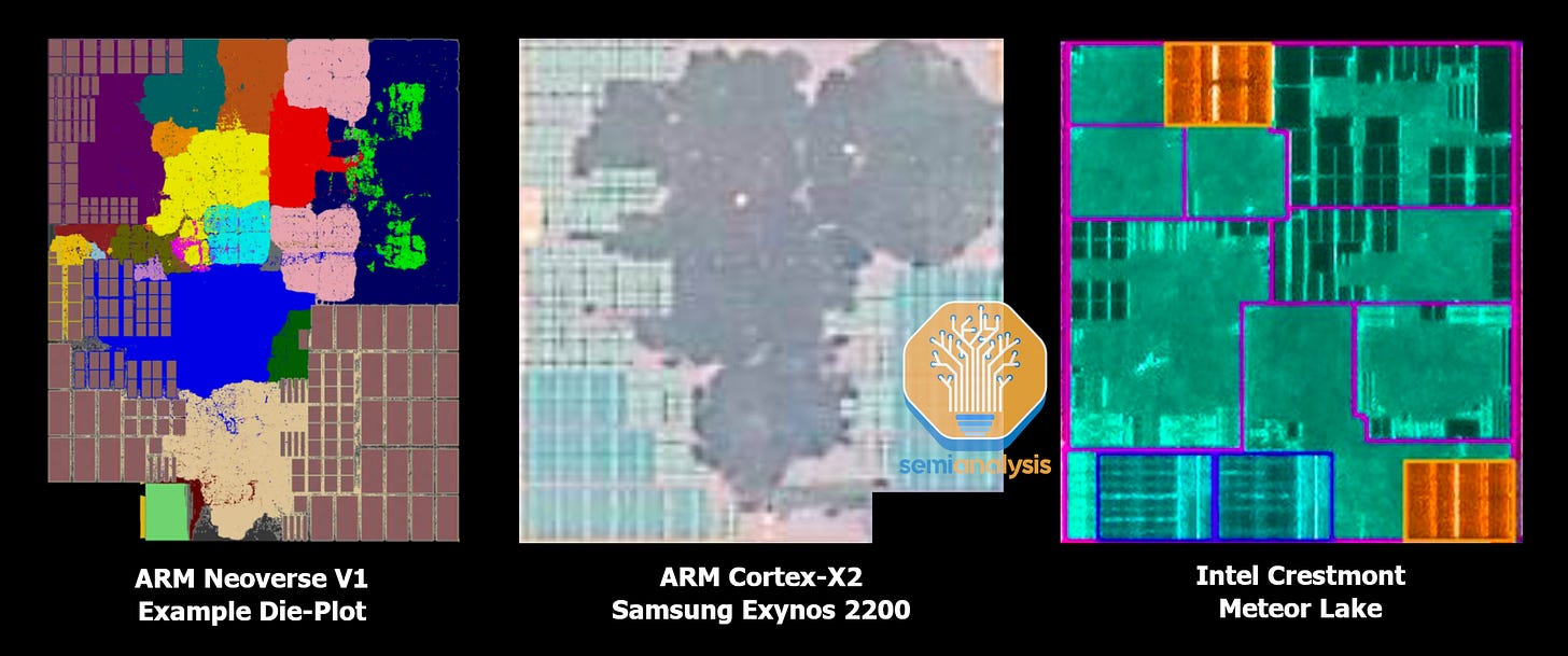
Zen 4c looks so different due to a flatter design hierarchy with fewer partitions. With such complex core designs with several hundred million transistors, it makes sense to split the core up into distinct regions in a floorplan so that designers and simulation tools can work in parallel to speed up Time to Market (TTM). Any engineering changes to a circuit can also be isolated to a sub-region without having to redo the placement and routing process for the whole core.
Intentionally separating timing critical regions can also help with routing congestion and achieving higher clock speeds from less interference. We see ARM’s Neoverse V1 and Cortex-X2 cores without hard partitions between logical regions, with placement packed as tight as possible. The regions appear homogenous when looking at the physical die. On the other hand, we see Intel’s Crestmont E-core with many visible partitions, with the boundaries highlighted in purple.
As seen in our Zen 4 core annotations, there are numerous partitions for each logical block within the core, but this is drastically reduced in Zen 4c with just 4 partitions (L2, Front End, Execution, FPU). By merging those partitions from Zen 4, the regions can be packed closer together, adding another avenue of area saving by further boosting standard cell density. One can say that AMD’s Zen 4c ‘looks like an ARM Core’.
The final method of area reduction is by using denser memory. Zen 4c has a reduction in SRAM area within the core itself, as AMD has switched to using a new type of SRAM bitcell. Pictured is a diagram of an 8T SRAM circuit with 8 transistors. The 4 transistors in the middle are used to store 1 bit of information, while 2 pairs of access transistors feed 2 pairs of wordlines and bitlines. High-performance Out-of-Order cores have multiple functions that read and write from the same piece of memory, so these 8T dual-port bitcells are used. These take up more area and require double the signal routing resources compared to denser 6T single port bitcells.
To save area, AMD has replaced these 8T dual-port bitcells with a new 6T pseudo dual-port bitcell developed by TSMC.
A 4.24GHz 128X256 SRAM Operating Double Pump Read Write Same Cycle in 5nm Technology, Z. N. Zhang et al, TSMC, Taiwan
A high speed 1R1W two port 32Kbit (128X256) SRAM with single port 6T bitcell macro is proposed. A Read-Then-Write (RTW) double pump CLK generation circuit with TRKBL bypassing is proposed to enhance read performance. Double metal scheme is applied to improve signal integrity and overall operating cycle time. A Local Interlock Circuit (LIC) is introduced in Sense-Amp to reduce active power and push Fmax further. The silicon results show that the slow corner wafer was able to achieve 4.24GHz at 1.0V and 100 degree Celsius in 5nm FinFET technology.
TSMC will be presenting further details on this new bitcell at VLSI 2023 in June, which SemiAnalysis will be attending. From the description, we see that TSMC is able to simulate a dual-port bitcell by doing a sequential read-and-write operation in the same clock cycle. While this is not as flexible as two independent access ports, the area reduction is significant enough for AMD to adopt this technology for Zen 4c. We will see more of these area-saving techniques going forward as SRAM area scaling flatlines.
Next, let’s zoom out and cover performance, cost, ASP, hyperscaler order switching, volumes, and adoption in non-datacenter enviroments.


