2022 NAND – Process Technology Comparison, China's YMTC Shipping Densest NAND, Chips 4 Alliance, Long-term Financial Outlook
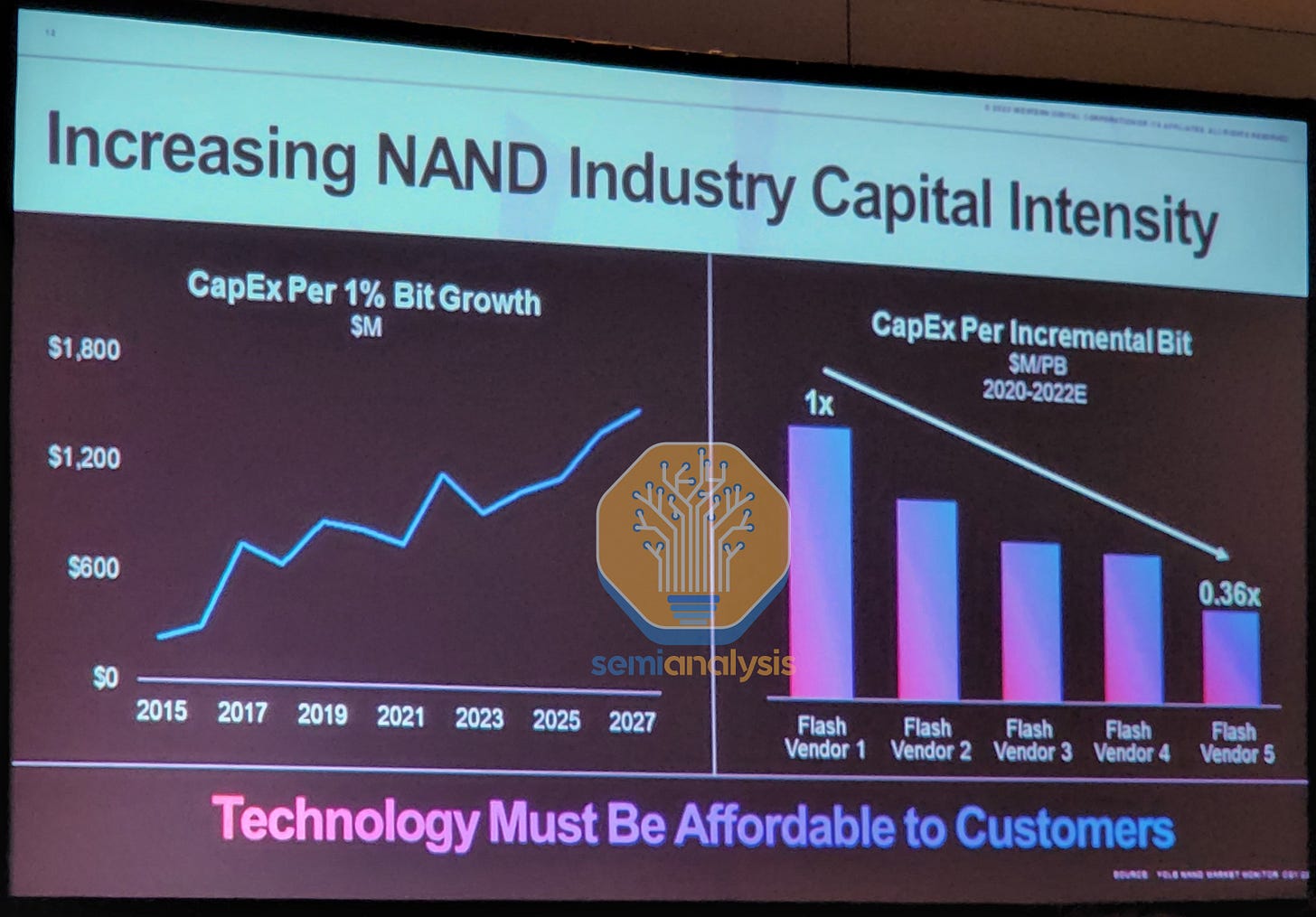
NAND is a market with fierce competition and a relentless march of progress. The number of bits of NAND manufactured and shipped has grown at a pace of 30% to 35% every year, doubling every 2 to 3 years. The initial take would be that this requires a large amount of capital dedicated to new equipment, but the NAND industry has only spent from $15B to $20B on wafer fabrication equipment every year from 2017 to 2022 despite exponential growth. The cost to produce NAND has fallen rapidly.
Similar cost scaling improvements were common decades ago in other semiconductor technologies such as DRAM and logic, but these sub-industries would consider this rate of improvement alien in the post-Moore’s Law universe. Productivity increases have been primarily driven by improvements in Lam Research’s etch and deposition tools, and the process nodes manufacturers developed.
Historically, when the semiconductor industry has held such rapid innovation, many firms were left in the dust technologically. Industry consolidation occurred. Only a few strong players emerged. 3D NAND is in a similar place today, and the future economics of the industry are in flux. Intel sold their NAND business, and there is a large amount of turmoil at Kioxia and Western Digital.
In this report, we want to conduct a status check on process technology from Samsung, SK Hynix, Micron, Solidigm, YMTC, Western Digital, and Kioxia. The quick summary is that Micron, SK Hynix, and YMTC are racing ahead of the others. At the same time, Samsung has oddly fallen behind despite being the absolute leader in NAND technology just a few years ago. SemiAnalysis and Angstronomics compiled the table below. It has many nuances which will be explained in the report.
The biggest highlight is that China’s YMTC is now shipping the highest density 3D NAND. We are exclusively detailing specifications and details associated with YMTC’s newest process technology which they have intentionally been concealing in 1st party materials. This is similar to China’s SMIC, which did not disclose anything about its 7nm process technology. We also have information on potential sanctions/tool ban, the Chips 4 Alliance, and existing NAND fabs from SK Hynix and Samsung in China.
Lastly, we will also detail the NAND industry's financial prospects, including the long-term through-cycle profitability and free cash flow margins. This includes discussing the shaky future of Western Digital and Kioxia in the NAND business and a rumored buyout offer.
Potential China Tool Bans, Chips 4 Alliance, Existing Fabs In China
Before we move on to the technology and business section, we want to discuss the geopolitical happenings. There have been numerous reports about the US looking to ban 3D NAND tools from China. Last year, we wrote a report for a PAC which was distributed around Washington that floated the idea and its impacts. The basic story is that Lam Research and other semiconductor manufacturing equipment firms could have tools blocked from being exported to China. If these tools were blocked, it would stop the current 3D NAND expansions by YMTC as well as Samsung and SK Hynix.
The Chips 4 alliance is a potential alliance between the US, Japan, Taiwan, and South Korea. These 4 countries encompass the majority market share in every facet of the semiconductor supply chain. This includes supply chain inputs such as wafer substrates, photoresist, CMP slurry, and etchant gas. These nations also represent most wafer fabrication equipment, memory companies, foundries, and IDMs.
The alliance’s goal is to increase supply chain security; cooperate on research and development; and workforce development. The clear undertone is that this alliance will be used to contain China’s rapid rise in the semiconductor industry. South Korea is publicly being tepid about joining the alliance. Our understanding is that the South Korean administration and the public have swung to being very hawkish against China, so this could just be posturing.
If South Korea elects not to join the Chips 4 alliance, we are hearing the US may even try to force their hand. This could be achieved by banning the shipment of 3D NAND tools to China. Samsung and SK Hynix both have NAND fabs in China. Alongside YMTC’s capacity, our data shows that China totals 24% of global NAND production in Q3 2022. Furthermore, SK Hynix also has DRAM fabs in China. The US tool ban would effectively force South Korea to cooperate less with China on semiconductors as those fabs cannot be expanded.
SK Hynix is in a very tough place. They were wooed into China with significant subsidies for DRAM and NAND fabs, but now they face difficulties upgrading production. Memory relies on utilizing the latest technology to produce at the lowest cost per bit. With DRAM, SK Hynix’s latest DRAM node uses EUV lithography, which China cannot import. This means their DRAM fab will slowly fall behind. In a few years, it would be uncompetitive in cost per bit manufactured compared to SK Hynix fabs outside of China. SK Hynix has plans to convert the existing DRAM fab to 3D NAND in the future as 3D NAND tools currently have no export controls. This would be a costly capital transition, but one that has been planned for and expected for years. These plans all change if the 3D NAND tool ban occurs.
Both Samsung and SK Hynix will be in a very tough place if they cannot import 3D NAND tools into China. They could reconfigure existing facilities for new nodes, but a large portion of the productivity improvements in 3D NAND manufacturing have come from new or upgraded tools from Lam Research. Banning 3D NAND tools from China would sink YMTC’s future expansions and make it costly for Samsung and SK Hynix to continue their operations in China over the long term. If the US follows through on this ban, it could give Samsung and SK Hynix subsidies in the US to temper the blow.
YMTC
YMTC has been very coy with their new generation of NAND, marketed as Xtacking 3.0. They will not officially say the layer counts anywhere. The official line does not go beyond marketing Xtacking 3.0 as the industry’s densest 1Tb TLC NAND. We imagine YMTC wants to hide this technical detail because they fear US sanctions. Many allegories can be drawn to SMIC’s concealment of their 7nm technology and high volume ramp of 14nm. It makes sense that YMTC is being coy in that context.
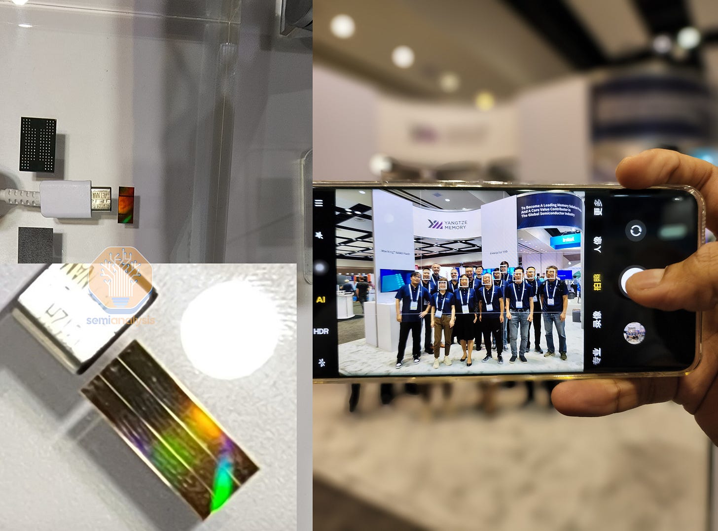
YMTC has developed some stellar process technology. SemiAnalysis can exclusively detail specifications that YMTC did not publish. First, Xtacking 3.0 is the densest commercial 1Tb TLC NAND at 15.2Gbit/mm2. Second, an employee told us it is “more than 230-layers”; we believe 232-layers. Third, it is comparable to Micron’s 232-layer NAND in performance, utilizing a similar 6-plane architecture with a 2.4Gbps data rate. Lastly, it is already shipping to partners.
We established these facts by measuring a physical die with the virtual help of Angstronomics. Having access to the physical die also allowed us to confirm that it is 6-planes. We also further details by talking to employees on and off the record. We spent so much time with them at the booth that they even asked us to take the company photo. We found their new NAND packaged in SSDs at a 3rd party Taiwanese company’s booth. They were happy to tell us some other details, including shipment timing.
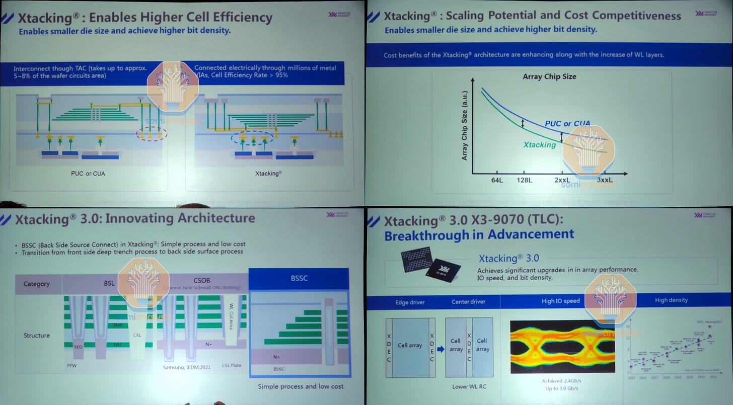
In the future, we may do an entire piece on their innovative technologies such as hybrid bonding CMOS over array, center driver XDEC, and the transition from Front Side Deep Trench process to a Back Side Source Connect (BSSC). YMTC also has plans to implement further logic for in-memory processing, including neuromorphic type computing with their stacked CMOS technology.
YMTC is not just a copycat with trailing edge technology like many erroneously perceive Chinese semiconductor companies on the leading edge. They are building their own innovative and unique product. While they rely heavily on the over 24 billion dollars of government subsidies, process tools from Lam Research, and licenses of critical technology from Adeia (Xperi), they are running ahead of other players in NAND with homegrown innovation.
YMTC is still behind on yields, but they have been rapidly improving them. In a couple of years, we have no doubt that YMTC will be cost competitive with even the best in the industry. They will structurally change the NAND industry. Firms that do not possess a durable advantage in technology or large subsidies will face an apocalypse regarding their future business viability. YMTC’s 2nd fab is nearly full of tools, and the 3rd fab is under construction. Funding for the 4th fab is allegedly underway with construction starting as early as the middle of next year. Each of YMTC’s fabs will have 100,000 wafers per month output.
Kioxia and Western Digital
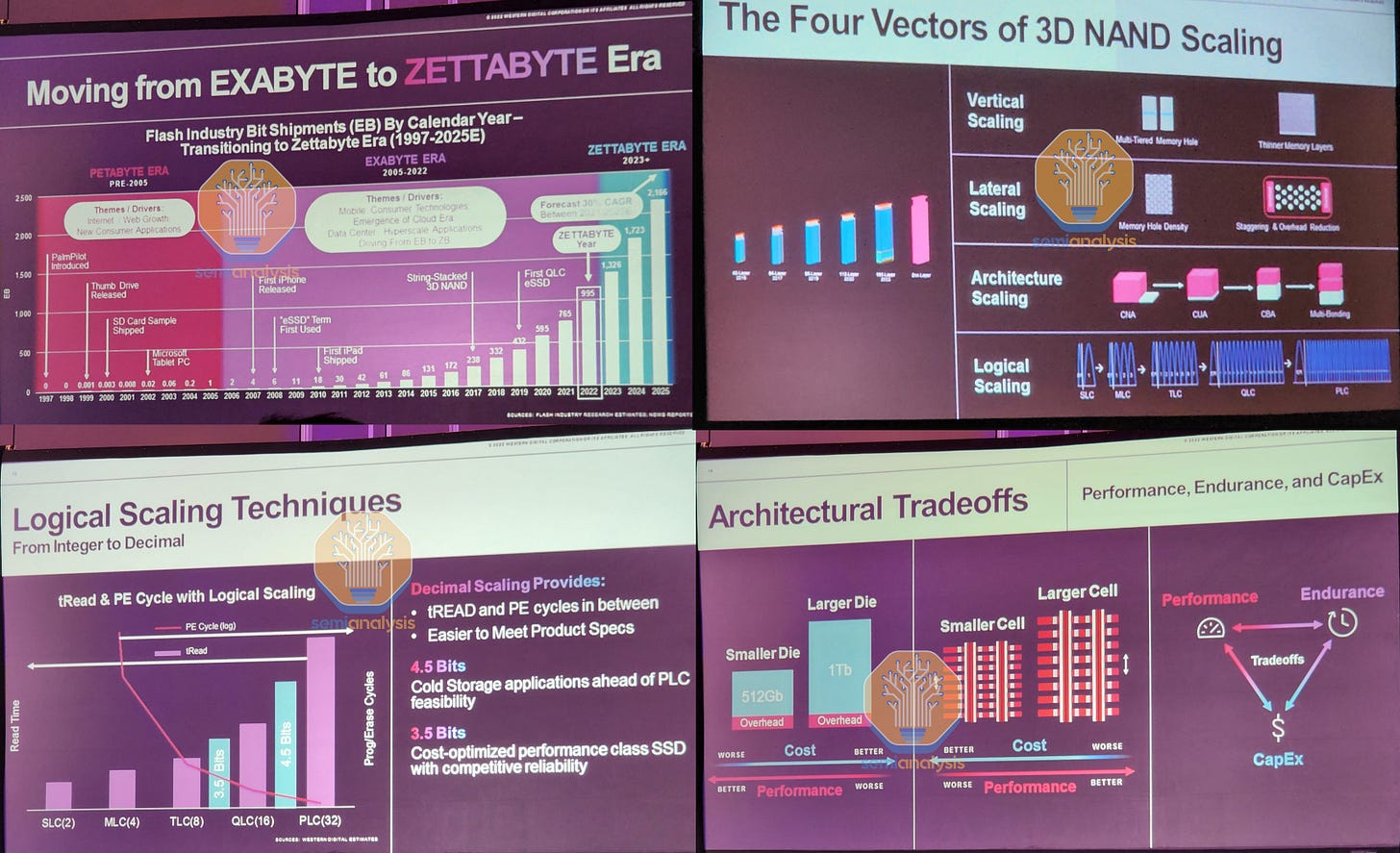
Kioxia and Western Digital cooperate on manufacturing and technology development for 3D NAND, so they are grouped together. They estimated that a Zettabyte of NAND would ship in 2022. Their Flash Memory Summit presentation covered some of the tradeoffs with 3D NAND scaling. There are 4 main vectors to scaling, vertical scaling, lateral scaling, architecture scaling, and logical scaling.
Above is an interesting slide regarding scaling from SLC, MLC, TLC, QLC, and PLC. As more bits are stored in a cell, the read latency increases, and the program erase cycle endurance decreases. Kioxia and Western Digital are exploring using 4.5 bits per cell or 3.5 bits per NAND cell to increase density and improve cost without sacrificing as much latency and endurance.
In 3D NAND, engineering choices often fall on a spectrum of performance, cost, and endurance. Larger capacities are more cost-effective but less performant for an SSD with an equivalent capacity. Larger cell sizes perform better but cost more to fab due to having more difficulties scaling to higher layer counts.
PCIe was stuck on 3.0 for many years, but the generational improvements have accelerated in recent years. This has led to many innovations to fully saturate the available bandwidth. Kioxia and Western Digital say the interface bandwidth for their NAND has increased by 30% each generation. Furthermore, they introduced asynchronous independent plane read, which allows reads in each plane to be packed more effectively (most competitors introduced this or will do so in their generation). Random read performance has improved significantly as a result of these innovations.
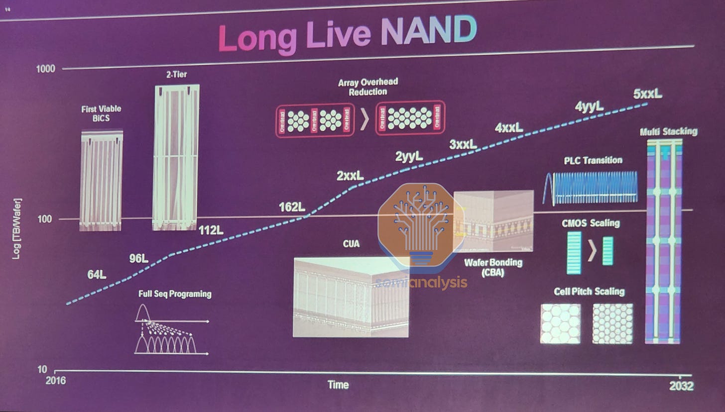
The Western Digital and Kioxia roadmap includes scaling layers as well as non-layer count related technologies. Wafer bonding is listed as the next technology to be adopted as a means of increasing cell array efficiency. This is the technology YMTC is on their third iteration of with Xtacking 3.0. PLC NAND is also being considered. Western Digital told us that they even have been experimenting with as high as 7 bits per cell (128 voltage levels) in their labs. It exists in their labs but requires extremely low temperatures maintained by liquid nitrogen.
Kioxia and Western Digital are the only firms with PLC charge trap memory on their roadmap. CMOS scaling and cell pitch scaling are also on the roadmap. The last technology they discussed is multi-stacking. The CMOS array and multiple NAND arrays would all be stacked with a sequential hybrid bonding method. The cost improvements with this technology are theoretically minor, but the density gains would be massive.
Kioxia and Western Digital have also developed a 2nd generation storage class memory they market as XL-Flash-2. It remains to be seen if it will ramp in volume due to the higher cost, but it is significantly faster due to utilizing 16-planes and MLC NAND. This would only make sense for large-scale deployments on a lower latency CXL bus, but DRAM pooling/sharing is often favored for those workloads.
Kioxia’s and Western Digital’s business/financial situations will be discussed separately later in this article.
Samsung
Samsung has had the highest market share in NAND for a long time. They have historically led in many of the technology transitions, as seen in the history and timeline of flash memory. This technology lead existed through to their 128-layer technology, the world’s highest volume NAND process node.
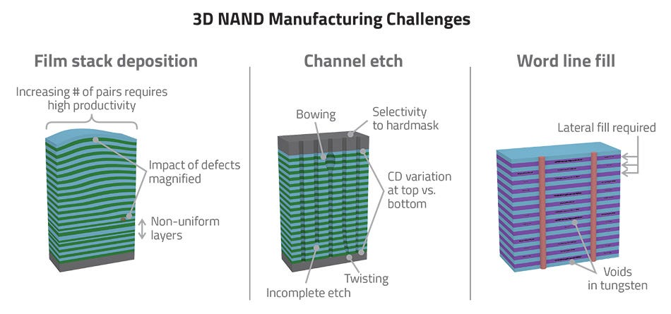
The most critical process step in 3D NAND is the high aspect ratio etch through many layers of NAND and subsequent deposition steps. While practically everyone in the industry uses Lam Research’s tools for most of these critical steps, Samsung is the only company that etches through more than 120 layers at once. Other firms utilize multiple decks on their greater than 100-layer NAND architectures, but Samsung 128-layer only uses 1. Solidigm, for example, uses 3-decks on their 144-layer NAND. Each deck additional increases costs.
Despite leading at 128-layer, Samsung has not shipped a new NAND process technology in years. Their 176-layer and >200-layer NAND process technologies have not been found in any SSDs by reverse engineering firms or teardowns. This is despite their claims of shipping 176-layer consumer SSDs in 2021. While the official reason is undisclosed, it most likely stems from process troubles induced by cultural issues. Samsung still states that the 7th generation V-NAND, 176-layer 512Gb TLC at 2Gbps, was a 2021 technology. They also note that 176-layer 1Tb QLC is coming soon. The 8th generation V-NAND is more than 200-layers. Samsung says it will be a 1Tb TLC die at 2.4Gbps, shipping in 2022. The 8th generation would be a lateral shrink, more layers, and a periphery shrink all at once. Samsung also put the 9th generation V-NAND in 2023. We are skeptical of their claims, given the status of the 7th generation V-NAND.
Samsung is in a precarious position where companies who were once behind are now racing ahead and starting to achieve better cost structures. Layer counts are not the end all be all of NAND scaling, and many other factors go into the final cost per bit. Based on our cost model, Samsung still has the 2nd most cost-effective NAND process technology due to its high capital efficiency and yields with the long-standing 128-layer process node. Our theory is Samsung avoided ramping their 176-layer NAND because it is less cost-effective than 128-layer due to moving to a 2-deck architecture.
If Samsung continues to delay its new process nodes, they risk slipping further behind. As an aside, many of the process engineers we spoke to at the Flash Memory Summit from competing firms were very confused about what’s happening with Samsung with NAND process node transitions.
SK Hynix and Solidigm
SK Hynix has been improving in relative positioning. They have ramped 176-layer TLC rapidly with 176-layer 1Tb QLC mass production in Q4. Our cost model has SK Hynix as the 3rd most cost-effective NAND process technology, and they may even swap places with Samsung soon.
SK Hynix 238-layer begins mass production in the first half of next year with a 512Gb TLC die. SK Hynix says the new NAND technology will produce 34% more bits per wafer, 50% faster IO speeds, 10% better program performance, and 21% better read power efficiency. This NAND is wicked fast at 2.4Gbps. Micron and YMTC are only planning 1Tb dies in their 232-layer count technologies, but SK Hynix can achieve the same speed with smaller 512Gb dies and only 4-planes instead of 6.
The future roadmap SK Hynix presented is very interesting. SK Hynix is saying they plan to continue with CMOS under Array NAND for 3 more generations after the 238-layer generation. In particular, the following xxx-layer NAND process will be a more significant layer count increase and a quicker transition.
SK Hynix has a horrible marketing name for their long-term innovations – 4D^2. These involve a shared bit line and more rows. Instead of cells being independent and storing 8 voltage levels for 3 bits per cell, they discussed using 2 cells in tandem to store more than 6 bits of data. The focus with all these technologies seems to be packing more bits per layer.
Turning gears to Solidigm (formerly Intel’s NAND business), the NAND architecture differs. Solidigm uses a floating gate architecture, and SK Hynix uses charge traps. SK Hynix plans to use their in-house charge trap for performance and mainstream, while the Solidigm will be used in value and HDD replacement sectors. Part of the terms of the deal between SK Hynix and Intel involved the process technology folks transferring over from Intel in a few years instead of immediately. The Solidigm Dalian China fab will run on Intel-developed process technologies for at least a few more years.
That next generation Solidigm floating gate node is 192-layers. We believe this is a 4-deck design with each deck with 48-layers for each deck. The cost-effectiveness of this process would be highly debatable with a TLC architecture. That cost disadvantage is mitigated by utilizing more bits per cell, an advantage the floating gate architecture has over the charge trap architecture. While most charge trap volume is TLC (3 bits per cell), the Solidigm nodes focus on QLC for volume.
The 192-layer QLC will come with a 1.33Tb die capacity. QLC has been plagued with poor performance due to having to accurately hold 16 voltage levels to store 4 bits per cell, but the new node claims to solve many of these issues. The 4th generation of QLC has some pretty-stellar claims with 2.5x faster program write time, 5x better random read, and 1.5x better read latency at the 99th percentile. These improvements would bring the Solidigm 192-layer QLC performance much closer to that of charge trap TLC.
The more exciting change is that the 192-layer process will be the first volume PLC NAND with a 1.67Tb die capacity. With PLC, the cell must be capable of accurately holding 32 voltage levels to store 5 bits per cell. This improves the number of bits manufactured per wafer by 25% but trades off performance. The performance hit is likely huge, given SK Hynix is pitching PLC NAND as an HDD replacement technology. As a fun stunt, the team at Solidigm ran the presentation off an external SSD, which utilized 192-layer PLC NAND.
Micron
Micron has been a rising phoenix in the NAND industry. A handful of years ago, they were tied to the hip with Intel in the IMFT joint venture. They used the floating gate architecture, which is inferior in cost-per-bit or performance compared to charge trap. They were also lagging a couple of years behind Samsung in DRAM process technology.
Micron made some radical changes, and now they are a leader in the memory industry. Sanjay Mehrotra was the co-founder and CEO of SanDisk, which was sold to Western Digital for $19B. He was appointed as Micron’s CEO not too long after. The Intel joint venture (IMFT) was dissolved, and the NAND architecture transitioned from floating gate to charge trap. 3D XPoint memory development was also halted.
Some underlying process and culture problems at Micron were fixed. Micron went from among the worst cost structures in 3D NAND to the best cost structure in 3D NAND. Likewise, they went from the lowest density and most costly to fab per bit DRAM to shipping the densest DRAM with the 2nd best cost structure.
Most of Micron’s capacity is 176-layer, and they are ramping and shipping 232-layer NAND. Micron’s strategy has been to keep wafer starts mostly the same and focus on much better process technologies to grow bit shipments. This has allowed them to keep CAPEX down but still maintain market share. That strategy may shift as greenfield investments totaling $40B could happen in the US thanks to the Chips Act.
Micron’s 6-plane 2.4Gbps 1Tb TLC 232-layer NAND was at multiple SSD and controller company booths. These 3rd party firms told me they expect the ramp to be rapid and 232-layer to be the majority of Micron’s volume next year. There are some issues with the being on the borderline of sub-scale, but more on that later.
Long-Term Financial Outlook and The Future of Western Digital and Kioxia
The long-term free cash flow margin of the NAND industry as a whole, as well as the future of Western Digital and Kioxia specifically, will be discussed in the subscriber-only section. One scoops we have is related to an informal buy offer for Western Digital’s NAND business.


