Austria’s Silent Monopolies On Advanced Semiconductor Manufacturing – EV Group and IMS Nanofabrication
All advanced logic, DRAM, NAND, and CMOS image sensor fabrication is dependent on Austria
The semiconductor supply chain is a smattering of critical dependencies that would take a decade and trillions of dollars to replicate completely. The typical examples of these dependencies are TSMC in Taiwan and ASML in the Netherlands, but there are many more bottlenecks throughout the industry. Those familiar with the semiconductor industry could easily rattle off another dozen companies just as critical to the global semiconductor supply chain. This list would include well-known firms such as Samsung, Intel, Cadence, Synopsys, Texas Instruments, Qualcomm, Broadcom, Tokyo Electron, Applied Materials, and Lam Research.
Beyond this list, so many unspoken segments of the semiconductor supply chain are geographically concentrated. These underappreciated dependencies stretch from chemicals to equipment to fabrication to packaging to IP to design to chips. To demonstrate just how concentrated and widespread the supply chain is, we want to highlight two firms in Austria. Austria is not known for semiconductors and is rarely discussed in supply chain security and geopolitics.
Despite this lack of notoriety, Austria’s EV Group and IMS Nanofabrication are quietly critical for all advanced semiconductor manufacturing. Every advanced logic, DRAM, NAND, and image sensor fabrication company relies on products from these two firms. Through these two firms, Austria’s market share is 82% in wafer bonding and over 95% of production multibeam mask writers. Finding replacement suppliers would require considerable time to achieve parity in technology and supply chain scale.
IMS Nanofabrication
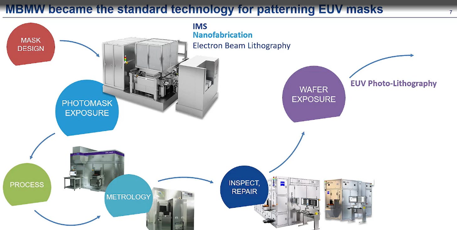
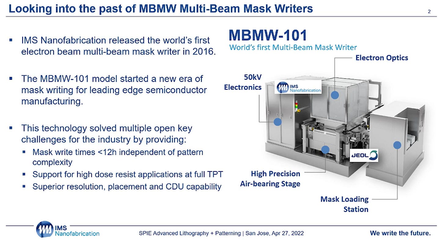
IMS Nanofabrication was founded in Vienna in 1985. They skated along with exciting research but no impactful products for a couple of decades. In 2009 they received an investment from Intel due to the promising nature of their multi-beam direct writing programable electron beam system. Eventually, Intel even acquired the firm as they released the first commercial multi-beam mask writer in 2016. This product and its derivatives are required for all process nodes beyond 7nm.
EUV lithography is seen as the biggest bottleneck for advanced semiconductor manufacturing, but these more than $150 million tools are paperweights without photomasks. A decent metaphor is that photomasks can be thought of as a physical stencil that lithography tools require to pattern layers of a chip. In turn, IMS Nanofabrication’s multi-beam mask writers can be considered the stencil drawer. Much like in the years of the printing press or block printing, a master printer would meticulously create the base design that all prints would come from; the mask writer helps create the mask set, which is then printed on numerous final chips.
Multi-beam mask writers are actually more precise and accurate than EUV lithography tools, but they are incredibly slow, which is a significant reason why they are used only for creating the mask set. IMS Nanofabrication has a competitor in NuFlare (Toshiba), but NuFlare’s tools are less precise, and slower. Furthermore, their multi-beam mask writers are only starting to enter the market many years after IMS Nanofabrication. Over 98% of production EUV masks have been fabricated using IMS Nanofabrication’s multi-beam mask writers.
Each individual chip design comes with a set of masks that can cost as much as $50 million on a 3nm class node. New masks are not only required for new designs but also for existing designs. Masks begin to have defects over time; as such, they need to be repaired, or new ones must be made to replace the aging ones.
Without IMS Nanofabrication’s mask writers, all EUV process technologies would grind to a halt. EUV is used in all Intel and TSMC process nodes beyond 7nm. EUV is also used in all of Samsung’s logic process technologies since 7nm. Samsung also utilizes EUV in their latest two generations of DRAM process technology. Furthermore, SK Hynix uses EUV in their latest generation of DRAM process technology. Micron plans to introduce EUV into DRAM. These 3 companies account for more than 90% of DRAM production.
While leading-edge logic is critical, DRAM is used in every electronic you can think of, so the criticality of IMS Nanofabrication and Austria on the semiconductor supply chain should not be understated.
EV Group
EV Group is a private firm based in Austria, so most folks likely haven’t heard of them. They are a supplier of semiconductor manufacturing equipment for mask alignment, nanoimprint lithography, photoresist racks, wafer cleaning, and inspection and metrology. While they have varying success in these markets, the market that EV Group outright dominates is wafer bonding. They have 82% market share in this type of tool, with the next closest player, Tokyo Electron, only having 17% market share.
Their dominance in this field means that most CMOS image sensors fabricated by Sony, Samsung, and Omnivision utilize their technology for backside illuminated CMOS image sensors or hybrid bonded image sensors. Nearly every smartphone, automotive, and security camera sensor touches an EV Group tool.
Furthermore, their technology is used in China’s YMTC fabricates. EV Group’s wafer-on-wafer hybrid bonding tools are critical to YMTC achieving the highest cell array efficiency in the industry. This use of hybrid bonding for NAND is also on the future roadmap for SK Hynix, Kioxia, Western Digital, Samsung, and Micron.
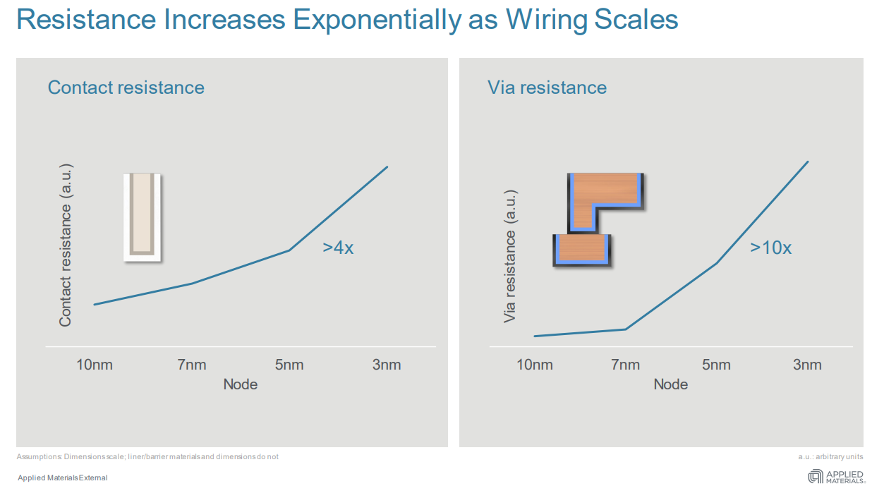
In addition to image sensors and NAND, wafer bonding is critical for leading-edge logic. The 2nm and on-process nodes will require wafer bonding tools. On-chip interconnects have become the major limiting factor for scaling to future process nodes. The resistance of contacts and vias has grown exponentially, limiting the power consumption and performance improvements when shrinking to the latest process nodes.
Over the last few years, mountains of research from leading firms such as IMEC, Intel, TSMC, and Applied Materials have been poured into breaking this bottleneck. A solution has been found with these firms all agreeing that backside power delivery networks are the way forward.
Currently, the transistor layer (front-end) is fabricated, then the contacts, then the back end, which connects all the transistors together and out of the chip to the external world. This has a few problems: power and signal must be routed in the same interconnect stack.
Backside power delivery network seeks to solve this by adding a 2nd interconnect layer for power delivery on the other side of the transistor layer. The signal and power delivery interconnects can be separately optimized for their specific task. Intel plans to introduce this technology at their 20A node in the 2024/2025 time frame, and TSMC plans to introduce it as an optional part of their 2nm node in the 2025/2026 time frame.
We explained the process flow and technology in February.
The process flow of building the transistor layer, building the signal interconnects, bonding to a wafer, then flipping the wafer, revealing nano TSVs, and creating the power delivery network.
This process flow at Intel and TSMC will rely heavily on EV Group’s wafer-on-wafer bonders.
In the future, all midrange and high-end CMOS image sensors, all NAND flash memory, all DRAM memory, and all advanced process technology beyond 7nm will rely heavily on wafer-on-wafer bonding technologies from Austria’s EV Group and multi-beam mask writers from Austria’s IMS Nanofabrication.
In the age where semiconductors are highly politicized between the potential Chips 4 Alliance and China, we find it humorous that Austria could singlehandedly bring the semiconductor supply chain for NAND, DRAM, logic, and CMOS image sensors to its knees if they wanted to.
This is a hypothetical situation, but it’s drawn out to demonstrate that the semiconductor supply chain could not operate without many countries. The US’s Chips Act or even China’s $250B in semiconductor subsidies over the next 5 years will not create an insourced supply chain. We like to say – trillions of dollars and a decade, and MAYBE you can achieve supply chain security for semiconductors.
SemiAnalysis is a boutique semiconductor research and consulting firm specializing in the semiconductor supply chain from chemical inputs to fabs to design IP and strategy.


