Beyond Advanced Packaging: Lightmatter Passage Chiplets Co-Packaged On Optical Interposer
But will products utilize this in volume?
Lightmatter made a big splash a couple of years ago by presenting an AI accelerator, Mars, that rethought the paradigm of how electronics compute and move data. They presented a processor that used photonics for compute. This chip promised multiple orders of magnitude improvement in latency, bandwidth, and power. This ultimately was unsuccessful due to the rigidity of the software and compute structure involved with the chip.
Lightmatter has created a 2nd generation of this AI compute product called Envise, but that is not the focus of today’s post. We want to share what Lightmatter presented on their newest product, Passage. We are simultaneously physically attending SPIE Optics and Photonics as well as virtually attending HotChips, so if you are here at SPIE Optics and Photonics or in San Diego this week, let us know, we would be happy to meet up.
The summary is that Lightmatter looks to break the constraints of advanced packaging and IO with Passage.
The problem size in areas such as AI and HPC is growing exponentially, but Moore’s Law won’t be able to keep up.
As such, the industry has moved to using chiplets to put together larger packages to continue meeting computing demands. Breaking chips into many chiplets and exceeding the reticle limit (physical limit of a lithography tool’s patterning limit) will enable continued scaling, but this paradigm still has issues. Even with advanced packaging, the power costs of moving data out of chips will become a limiting factor. Furthermore, the bandwidth is still limited even with the most advanced forms of packaging.
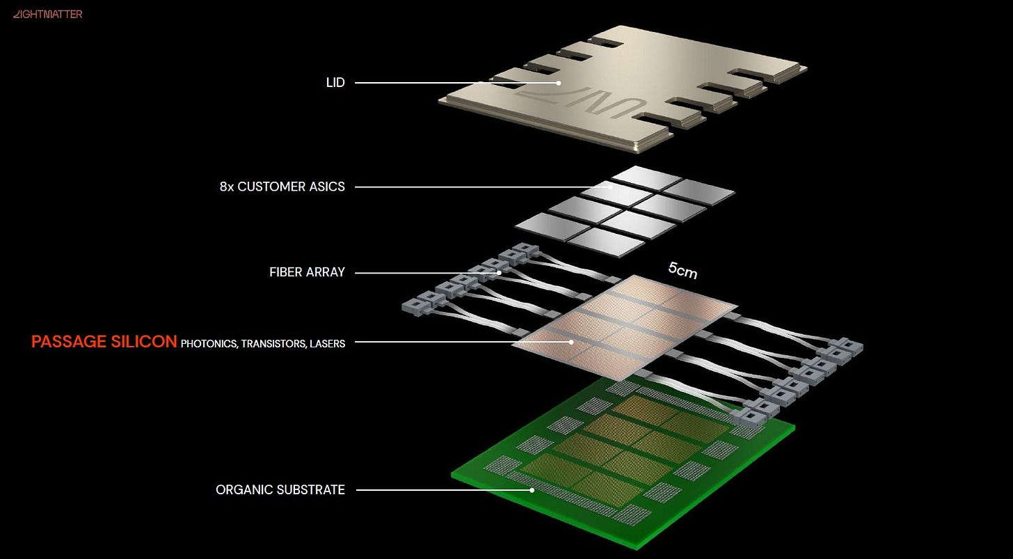
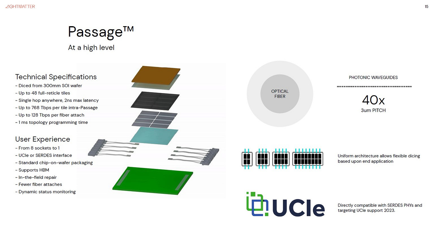
Rather than putting silicon on top of silicon, Lightmatter wants to flip the advanced packaging game on its head with Passage. Passage connects to 48 customer chips on an optical interposer. Passage is built on GlobalFoundries Fotonix 45CLO process technology. It is designed to connect many chips at very high bandwidth and performance. This optical interposer breaks bandwidth limitations by providing 768 Terabits per second between each tile and the possibility to scale to multiple interposers at 128 Terabits per second. This is a level of capabilities and scale that traditional packaging cannot achieve.
Optics has promised to solve the bottlenecks of electrical IO for decades. Technology has slowly progressed on that forefront. Pluggable optics, which Lightmatter dubs as Gen 1, has been used to connect switches within a datacenter for many years. Gen 2 and Gen 3 optics, where the optics are put on the same package or connected directly, is starting to come in networking switches and compute due to firms such as Intel and Ayar Labs. Lightmatter wants to skip straight to Gen 4 and Gen 5 with Passage.
Standard co-packaged optics like Intel and Ayar Labs are targeting has an order magnitude lower scale than the optical interposer solution that Lightmatter is using. The interconnect density is 40x higher because only about 200 fibers could be inserted into a single chip. Furthermore, the interconnect is completely static whereas Passage has a dynamically configurable fabric.
This optical interposer can perform switching and routing between chips. The entire interconnect can be reconfigured in under 1ms. Lightmatter says they can support all topologies such as all to all, 1D ring, Torus, Spine and leaf, and more. Passage’s switching and routing has a 2ns max latency between any chip to any other chip on the 48-chip array.
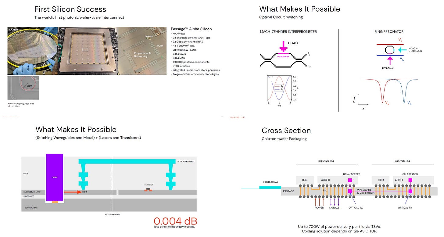
The switching is achieved by modulating colors with ring resonators and using Mach-Zehnder interferometers to guide them.
Lightmatter has A0 silicon of its photonic wafer-scale interposer and claims it uses less than 50 watts per site. Each site has 8 hybrid lasers driving 32 channels; each channel runs 32Gbps NRZ.
Lightmatter’s wafer-scale silicon photonics chip mostly uses silicon-based manufacturing techniques; it has many of the same constraints. Namely, the reticle limit of lithography tools. GlobalFoundries and Lightmatter get around this issue by stitching waveguides. Inter-reticle connections for the nanophotonic waveguides only has a 0.004 dB loss per reticle crossing. There is 0.5 dB/cm loss with the waveguides and 0.08 dB loss per Mach-Zehnder interferometer. There is also a 0.028 dB loss per crossing.
Lightmatter says that with UCIe, they can run the top spec of 32Gbps for chiplet to interposer interconnects. If direct SERDES are used, they believe they can run at 112G speeds. The customer ASICs are 3D packaged on top of the interposer. An OSAT would then assemble this final product. It can come in many variants, from 48 chips to smaller interposers with as few as 8 chips. The passage package has to also deliver power to the chips that are packaged on top. It does this by delivering up to 700W per tile with TSVs. Water cooling is required at this power level, but if the customer ASIC draws less, they can get away with air cooling.
Note that the claimed 768Tbps appears largely wasted. Their functionality seems to allow them to couple one input to one output. That leaves a large fraction of the interconnect idle. It would be needed in order for them to figure out the pathways that do not conflict. Those pathways are passive and waste little or no power when not used. The MZI elements go left or go right. No blending, no multicasting. One entry, one exit.
Lightmatter also gave an example of disaggregated memory design and multi-tenant architecture. They started their interposer can support any protocols, including CXL. The customer ASICs on top of the interposer can be air-gapped by reconfiguring the network, so passing data between specific chips would be impossible. The big question is whether and when products will come. This could just be vaporware, or it could be the future for high-end leading edge disaggregated server designs. Lightmatter has to woo other companies to build chips for this platform. These firms have to trust their expensive development with an unproven partner.


