Meta’s Alexis Black Bjorlin (VP of Infrastructure Hardware) discussed AI model scaling, training clusters, and co-packaged optics at the AI Hardware Summit today in Santa Clara. The presentation she gave was interesting not just because of the peek it gave into Meta’s infrastructure but also because of the commentary on future AI systems. In our opinion, this presentation also demonstrated that Nvidia is playing an entirely different ball game than most AI startups.
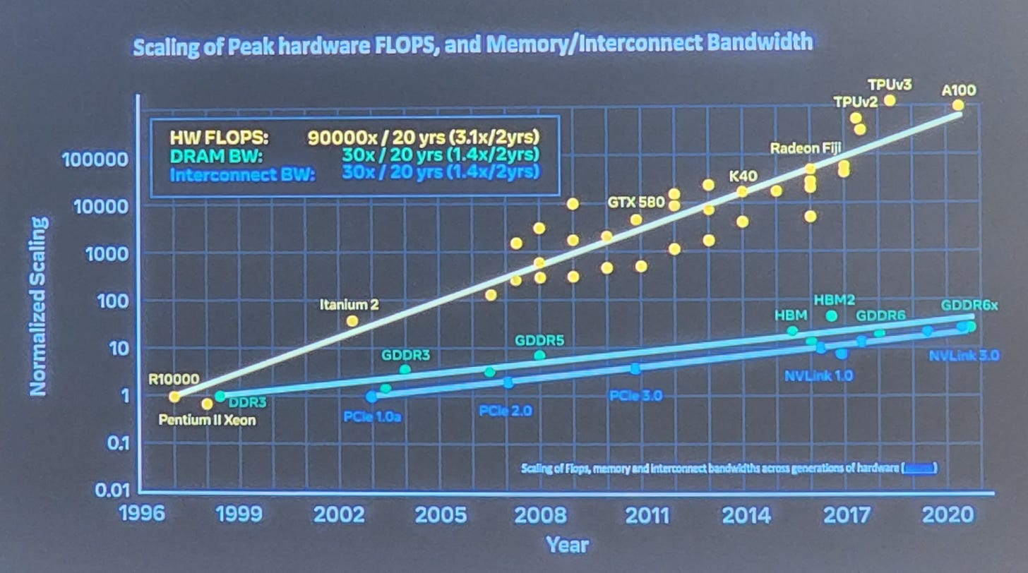
A common trend that we have discussed is the issue of DRAM scaling and network scaling. Both these trends are sides of the same coin; FLOPs are growing faster than we can get data in and out of a chip/package every generation. This isn’t a new phenomenon, but combatting the mismatch is becoming more and more difficult.
Meta spoke about these challenges regarding future model scaling. They commented that a large training cluster could be as much as 6 Megawatts today. They said that these training clusters would be 64 Megawatts in the future. The largest public supercomputers in the world are currently 20 Megawatts to 30 Megawatts. An incredible amount of power will be sucked down for training AI models. The costs to train these models will continue to soar.
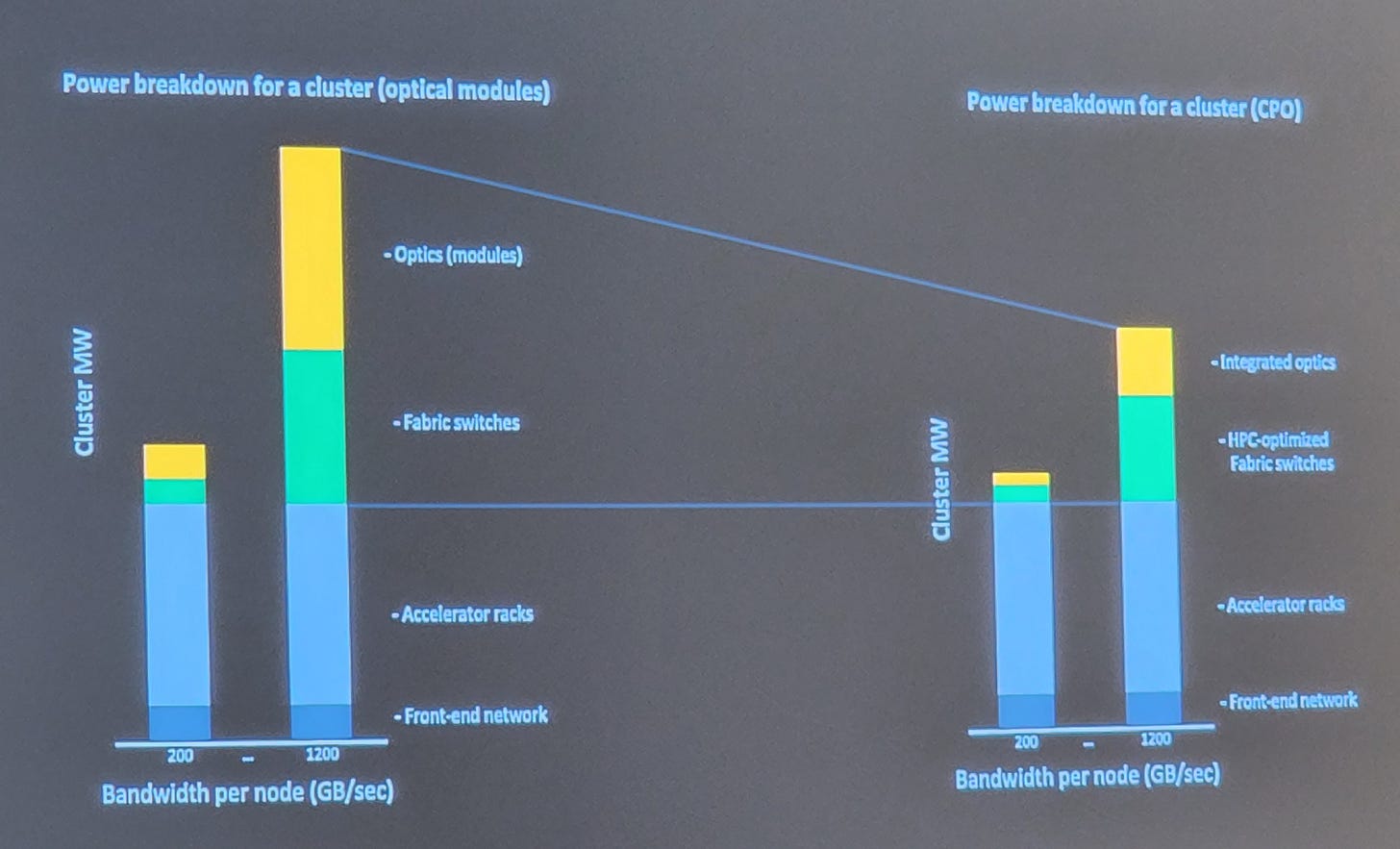
Meta presented a power breakdown for a training cluster. In the 200GB/s bandwidth per node accelerator generation, the accelerator servers consume most of the power. If we move a few generations forward from 200GB/s per node to 1200GB/s per node, networking balloons quickly to consume more than 70% of the power. Traditional optical modules and ethernet-based fabrics will not work. The world must move to HPC-optimized fabric switches with co-packaged optics. These problems are most apparent in the DLRM models that Facebook runs due to their massive extent tables.
This is where it’s obvious Nvidia is playing a different game. We’ve discussed Nvidia’s co-packaged optics research before. With Nvidia’s strategic investment in Ayar Labs and collaboration on co-packaged optics, Nvidia is poised to tackle this problem in a way most other AI startups have not considered. They also have partnerships with GlobalFoundries and TSMC for exploring co-packaged optics further.
Nvidia has built its own custom fabric that connects between many nodes. The primary purpose of this network is for memory sharing, sharding models across many nodes, and allowing for all-reduce operations on in-flight data.
We believe Nvidia will implement co-packaged optics on the next generation NVSwitch for inter-node communications. These systems should support ~4,000 GPUs in an interconnected an NVLink network. Meta said that in the 2025+ timeframe, each accelerator should have 1TB/s bandwidth to the rest of the network. With the model sizes for DLRS and MLPs extending to hundreds of billions of parameters, it will be difficult for the sea of competitors to keep up.
While other AI accelerators such as Graphcore IPU and Habana Gaudi offer direct links to other chips for inter-node communications to scale to hundreds or thousands of accelerators, most do not. Furthermore, most of these competitors don’t seem to have immediate plans for co-packaged optics or purpose-built switch architecture with in-flight compute capabilities. Even if these competitors’ compute architecture is multiple times more efficient while retaining flexibility and programmability, these firms also need in-house networking expertise.
Can an upstart beat Nvidia in software, compute hardware, and networking, all at once?
SemiAnalysis is a boutique semiconductor research and consulting firm specializing in the semiconductor supply chain from chemical inputs to fabs to design IP and strategy.


