ACM Research, China’s Most Successful Semiconductor Capital Equipment Provider, Wins At SK Hynix and Intel
Intel Buying Chinese Developed and Manufactured Tool Despite Alternative Suppliers And US Subsidies
ACM Research was founded in 1998 by Dr. David Wang focused on developing and selling stress-free copper polishing tools which were positioned as a competitor to chemical metal planarization (CMP). ACM Research’s (advanced copper materials) initial copper polishing tool did not find any success, but the company was able to sidestep the rocky beginnings and stay afloat due to their strong backing. The firm then pivoted and shifted focus to another area of the semiconductor capital equipment market, wafer cleaning.
At first glance, the wafer cleaning market sounds relatively simple, but that is deceptive. The cleanliness and purity levels required to continue the next step of semiconductor manufacturing cannot be understated. There are dozens of different cleaning steps involved in manufacturing a wafer and the target is an extremely fragile material. Patterns and features can easily collapse. For example, in 3D NAND, holes can be less than 1/20th the thickness of a human of a human hair. These holes are etched straight down with an aspect ratio of >25:1. Cleaning everything out of these holes is incredibly difficult. As FinFET transistors are formed, the various steps in the middle are even more difficult to clean. With gate all around nanosheets, the complexity of cleaning ramps even further.
Despite this, ACM Research has been able to carve a niche in the wafer cleaning business competing with multi-billion-dollar revenue companies such as Japan’s Screen and Tokyo Electron as well as the US based Lam Research. Furthermore, they have begun to expand upstream to electro-chemical plating and etch products as well. ACM Research achieved over $250M revenue in 2021 and has guided to hit as high as $405M this year. While most these sales are in China, ACM Research also has significant sales to Korea’s SK Hynix and is even qualifying at Intel as we speak!
Back to the history of ACM Research, after continuing to be funded by their backers despite their initial misstep with copper polishing tools, they opened a research facility in Shanghai. This was the start of their overt operation in China. If we fast forward to the present day, ACM Research’s research and development as well as production are all in China. There is a tiny amount of R&D in South Korea as well and a corporate “HQ” in California. All meaningful operations related to technology development and manufacturing are in China.
ACM Research’s first major customer was SK Hynix. SK Hynix opened a DRAM fabrication facility in Wuxi City, China after being wooed by large subsidies. It was SK Hynix’s first 300mm wafer fabrication facility and the site continues to receive large investments and subsidies to this day. This facility in China began to evaluate ACM Research’s tools and eventually they began to place orders at the turn of the decade. ACM Research first struck gold at SK Hynix with their SAPS single wafer cleaning tools.
The wafer fabrication industry was transitioning from batch wafer cleaning tools to single wafer cleaning tools. Batch wafer cleaning tools would dunk many wafers into a bath of circulating water or chemicals. As feature sizes shank, this was insufficient for the increased levels of cleanliness and purity that Moore’s law demanded. Single wafer cleaning tools would instead spray fluids (acids or ultra-pure water) through nozzles directly onto the wafer as it spins at high RPM. Here’s a video for those of you who need a visualization. Japan’s Screen first introduced rotating single wafer cleaning systems in 1983, but mass popularity of this type of tool took longer. Screen is still the leader in rotating single wafer cleaning due to their precise control and engineering around throughput, various nozzles types, chemical handling, minimization of waste chemicals, temperature uniformity, and humidity control.
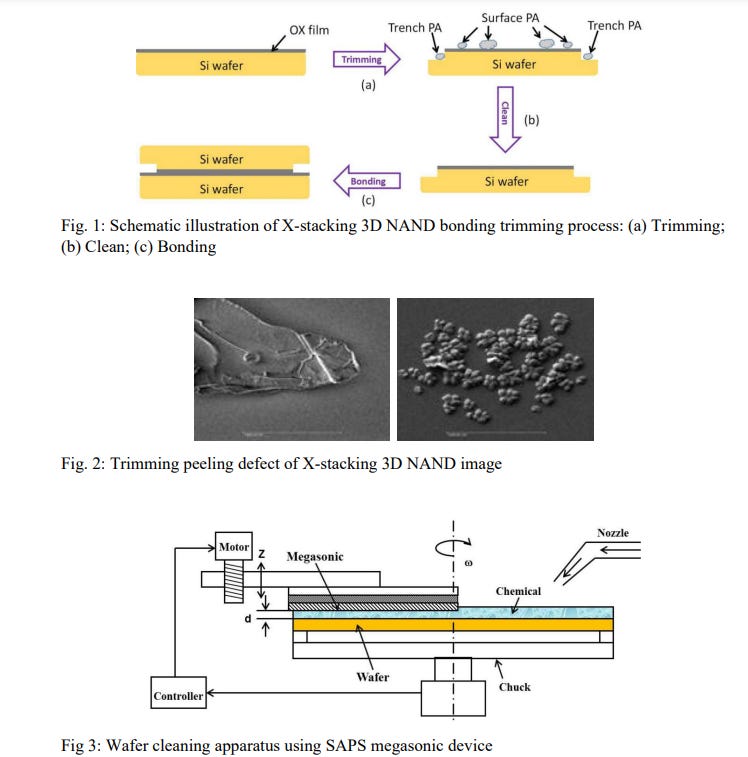
The ACM Research SAPS wafer cleaning tool is a single wafer cleaning tool, but with a key innovation. It utilized megasonic acoustic vibrations through the fluid bath to produce bubble oscillations which assisted with cleaning defects. Other manufacturers had introduced megasonics in the past, but a key issue was that as bubbles collapse, the resulting energy would often damage features on the chip. ACM Research also introduced space alternate phase shift (SAPS) which alternated the phases of the megasonic waves so that the energy delivered to the wafer was uniform and caused less pattern damage. Even with these innovations, SAPS is not currently used in any leading edge FinFET process by Samsung, Intel, or TSMC due to pattern collapse. ACM Research also has a similar technology known as TEBO (Timely Energized Bubble Oscillation) which has seen success in SK Hynix and YMTC NAND processes.
The state funded and subsidized Yangtze Memory Technology Corporation is the largest customer for ACM Research, but other Chinese state enterprises such as SMIC, HLMC, and CXMT are large customers as well. All of these firms have been proven to be directly working with the CCP for funding, research, and use of their chips in military applications. Much of these firms technology comes from American based companies too. For example, YMTC relies primarily of Lam Research tools for the fabrication of 3D NAND and San Jose based Xperi Corporation for Hybrid Bonding technology which YMTC has dubbed as “Xtacking.” ACM Research has published papers with YMTC regarding wafer cleaning for hybrid bonding as well. This could be an area where ACM Research and YMTC leapfrog Korean, Japanese, and American companies.
ACM Research is not only seeing success in wafer cleaning. They also have wins at packaging firms. The most notable win is with Tongfu Microelectronics who has been purchasing electro-chemical plating tools from ACM Research. As a reminder, Tongfu has a joint venture with AMD where AMD’s Epyc datacenter CPUs as well as client CPUs are packaged by Tongfu. Chips from the AMD Tongfu joint venture have even been shipped into the world’s fastest supercomputer, Frontier, which was built by the US Department of Energy.
The ACM Research electro chemical plating tool primarily competes with Lam Research’s Sabre 3D tools. This tool could potentially cause Lam Research to lose a large amount share as a large portion of electroplating for packaging applications is done in China.
While ACM Research argues they have unique differentiated tech, the vast majority of their sales come from the Chinese domestic market. They are subsidized, preferred as a domestic supplier, and undercut the competing products of Screen, Tokyo Electron, and Lam Research on price. The assumptions of market share in China is very high as a result. As long as ACM Research’s product is even somewhat close to foreign competitors, the domestic supplier status means they will win out in share. This is further emphasized by ACM Research’s own long-term estimates forecasting little to no sales for the rest of the world outside of mainland China.
ACM Research’s own presentations showcase they believe 42% of new semiconductor production facilities are in China. This lines up with SEMI World Fab Report and our own data. The top country in semiconductors has shifted every few decades, and ACM Research, much like the CCP, believes that the next decade will be China’s turn despite renewed initiative looking to level the playing field on subsidies from Taiwan, South Korea, Japan, Europe, and the US.
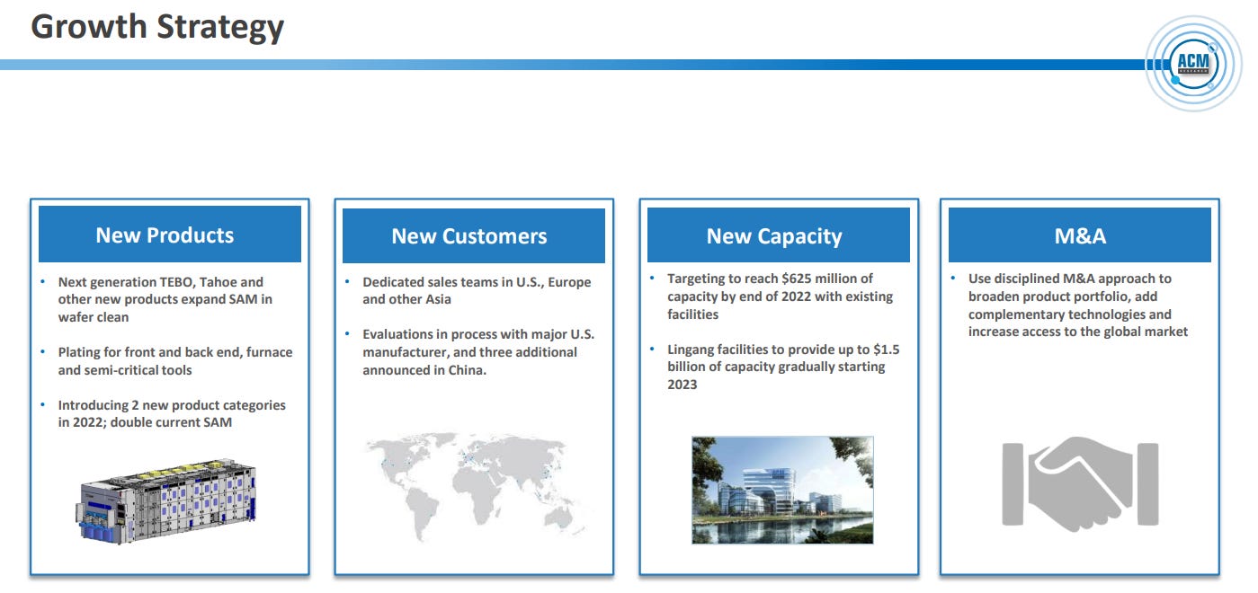
We were shocked when we learned that when ACM Research says “evaluations in process with major U.S. manufacturer,” they mean Intel. The same Intel that is currently begging the United States and European governments for subsidies due to East Asian dominance in the semiconductor industry. We confirmed with multiple sources including directly with ACM Research that Intel is in the process of qualifying an ACMR tool which was made in China for the Intel Oregon campus. The Oregon campus is subsidized by Oregon tax payers, so we wonder how these tax payers would feel if they knew they were helping pay for wafer fabrication equipment from China. Once qualified, it is very possible that Intel could utilize Chips Act government subsidies to import more tools into Oregon, Arizona, and Ohio for volume production despite the existence of Japanese and American alternatives.
ACM Research is projecting as much as $405M in revenue this year and they aren’t slowing down. They have begun to introduce photoresist stripping, CVD, and ALD products to compete more with Lam Research, Tokyo Electron, and Applied Materials. If successful, this would bust open a $30B sector of the wafer fabrication equipment market.


