Graphcore Announces World’s First 3D Wafer On Wafer Hybrid Bond Processor
Bow, Good Computer, and Wafer on Wafer Hybrid Bonding Analysis
Graphcore is announcing their newest AI accelerator, Bow. For the most part, the architecture is completely identical, except one massive change to system design. The introduction of 3D wafer-on-wafer stacking. They are the vanguard customer for TSMC’s wafer-on-wafer SoIC technology. We will do a deep dive on this packaging technology including the purpose, advantages, cost, process flow, and whose semiconductor manufacturing tools are utilized later in this article.
The wafer-on-wafer technology allows Graphcore to increase clocks and performance by up to 40% while maintaining similar costs versus the prior generation MK2. Graphcore says that this chip is currently shipping to partners including but not limited to the US Department of Energy and two cloud service providers, Cirrascale and G-Core Labs.
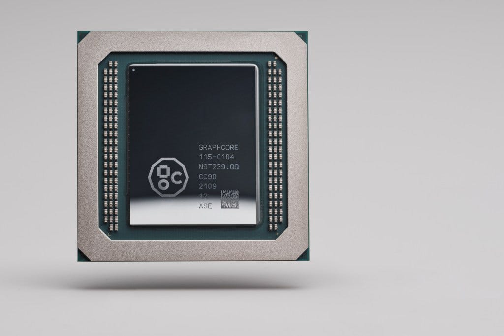
Those of you with a keen eye may notice this looks nearly identical to the previous generation IPU. That’s because the architecture, die size, and transistor counts are effectively identical. The processor is manufactured on the same TSMC 7nm node, and only contains some tweaks that enable hybrid bonding. End users will receive up to 40% performance benefit over the prior generation and up to 16% performance per watt benefit. Clock speeds were increased from 1.325GHz to 1.85GHz. The clock speed increase affects the raw flops of the chip as well as bandwidth delivered by the on-die SRAM.
The specs of the Bow Pod’s are identical in terms of CPU, memory, and inter chip bandwidth. The only changes are swapping out the prior accelerator for their new one, Bow. Graphcore is able to achieve this with 0 changes to the software due to the identical architecture. Graphcore emphasized there are no cost increases to end users. The lack of cost increases will be explained later in 3D packaging section. The 40% clock speed improvement translates to a 30% to 40% improvement in performance in their suite of workloads. The performance scaling from Graphcore’s 1st party benchmarks is pretty amazing given chip-to-chip bandwidth did not scale at all.
Despite the 40% higher clock speeds, performance per watt improves marginally. This is very surprising as the chip is still using the same process node. One would expect worse performance per watt due to the nature of exponential voltage-frequency curves. This relationship is shifted out due to power delivery optimizations from 3D wafer-on-wafer stacking.
The full software compatibility from the last generation is one of the strongest points about the Bow chip. Because the architecture is identical outside of software changes and the 3D stacking change, which is not exposed to the user, everything will transfer over perfectly. There are still some questions about the software ecosystem, especially relative to a competitor such as Nvidia.
Graphcore is claiming a massive time to train and TCO advantage, but every point from our previous article about Graphcore still applies.
They compared 16 of their TSMC fabricated 7nm 823mm^2 IPU’s vs 8 of Nvidia’s TSMC fabricated 7nm 826mm^2 A100’s. Comparing twice the silicon is quite disingenuous even if there is no HBM.
The Graphcore system has a much smaller memory capacity, especially in regard to high bandwidth pools. They used a small model as a comparison point to hide this deficit.
Graphcore specifically used 80GB A100’s rather than 40GB ones, which include a 1.5x price premium.
Graphcore specifically used Nvidia’s DGX systems which includes direct Nvidia support instead of an off the shelf system from an OEM. The comparable system from SuperMicro with 40GB A100’s would cost ~$125,000.
Despite these counterpoints, Graphcore’s improvements are quite sizable and Bow does likely beat Nvidia's A100 in TCO for many workloads. The only problem, Nvidia is already shipping their next generation Hopper GPU to select partners in higher volumes than Graphcore is shipping Bow. They will be launching the next generation Hopper GPU at GTC this month.
All Nvidia has to do in order to keep their advantage even in small models such as those in the MLPerf suite, is increase performance per GPU by up to 40% and efficiency by up to 16% at the same cost. Given Nvidia’s historical improvements and leaks related to performance and power, this seems very easy to achieve. Graphcore will still win in certain use cases, especially those with lower batch sizes, unless Hopper brings some major architectural improvements here.
Graphcore is also announcing the “Good Computer”, a system level approach which comprises of many servers and racks of their complete solution. It will have the full support of their popular SDK. This is very important as the AI training landscape is rapidly becoming a turnkey solution problem. Selling individual chips or even servers is not enough. The best AI training chips must be able to scale up and scale out to massive numbers of servers to tackle the largest multi-trillion parameter problems.
In terms of performance, this “Good Computer” exceeds that of even the Tesla Dojo supercomputer that Tesla announced but has yet to build. Only Fujitsu and Nvidia based supercomputers rival the “Good Computer” in terms of AI performance and capabilities. We are excited but remain skeptical of perfect strong and weak scaling given inter-chip bandwidth limitations. Graphcore stated future generations of their AI accelerators would tackle inter-chip bandwidth more directly.
The most exciting part of this chip is the 3D packaging. It is what enables the 40% clock speed improvement despite identical architecture and node at the same costs and improved power efficiency. A common issue with leading edge logic is the transient spikes. Smooth power delivery is critical and often the limiting factor preventing higher clock speeds. Graphcore demonstrated that by simply smoothing and improving power delivery, they can gain a huge clock speed increases without decreasing performance per watt.
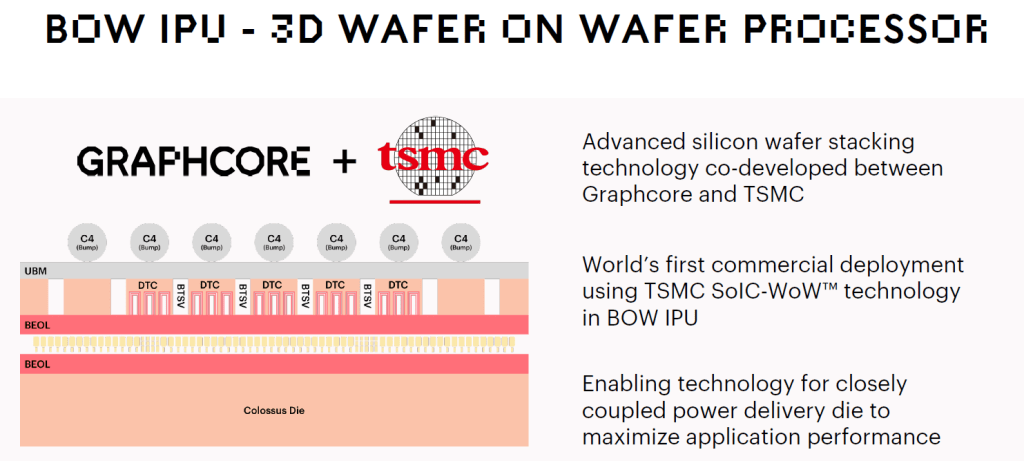
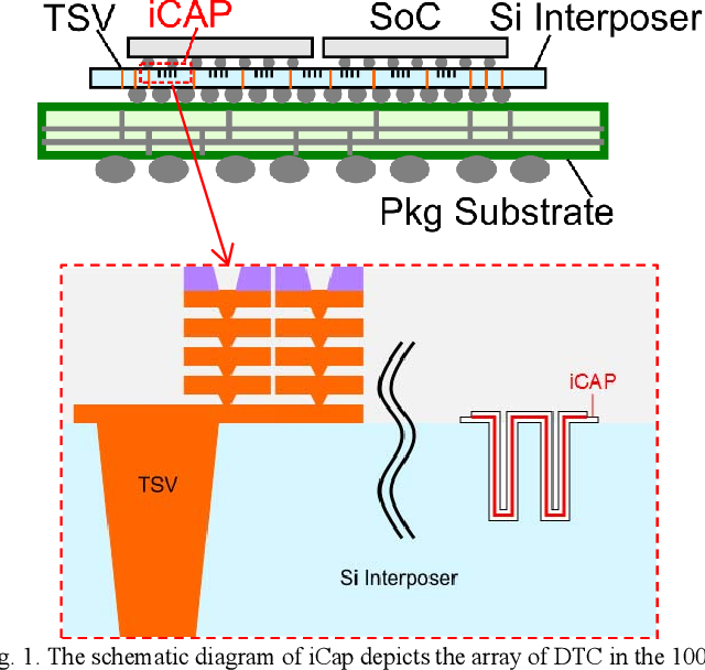
Graphcore achieved this by implementing a large number of deep trench capacitors on a second wafer and using TSMC’s SoIC wafer-on-wafer hybrid bonding technology to integrate the two. Most designs include some deep trench capacitors on die or even on package, but this is the first instance of 3D hybrid bonding for them. These embedded deep trench capacitors are similar to those found in prior DRAM processes. The packaging innovations enable orders of magnitude more deep trench capacitor capacity than any other high performance leading edge chip has had in the past.
We mentioned this in part two of our advanced packaging series, but TSMC’s chip-on-wafer-on-substrate technology (CoWoS) first introduced this technology to 2.5D packaging several years ago. Intel’s Foveros also offers deep trench capacitors on the base die. These capacitors sit on the base die and smooth the power delivery and increase stability by reducing the size of transient spikes. In laymen's terms capacitors are for energy storage. When the chip's current draw rapidly changes, they reduce voltage droop and smooth out the power delivery. The actual science behind it is more complex of course.
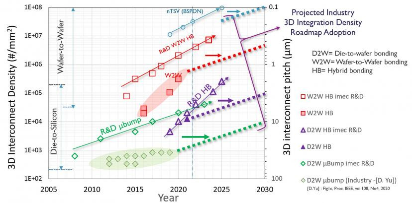
Graphcore is TSMC’s vanguard customer for this technology. The hybrid bonding process here is wafer-on-wafer rather than chip-on-wafer. This provides a huge benefit to density of packaging. AMD’s 3D V-Cache technology uses TSMC’s chip-on-wafer bonding at a 17-micron pitch for TSV’s. The wafer-on-wafer hybrid bonding technology is able to offer TSV’s at 1/10th the pitch. In other words, in the area that chip-on-wafer hybrid bonding is able to offer 100 TSVs, the wafer-on-wafer technology can offer 10,000.
In addition to improved density and therefore integration, the throughput of packaging is also increases sizably. Rather than having to pick up each polish, cut, clean, and place individual dies, wafer-on-wafer allows entire wafers to bonded at once. This greatly improves throughput and therefore costs. Any yield issues are solved architecting higher repairability of the design.
Sony’s image sensors and YMTC’s NAND also use wafer-on-wafer hybrid bonding technologies. TSMC’s wafer-on-wafer technology is quite different than the Xperi DBI, but we will save that discussion for our deep dive on hybrid bonding which will be released next week. Subscribe to the newsletter so you don’t miss this.
The process for TSMC’s wafer-on-wafer hybrid bonding is very interesting as starts off as a fusion silicon oxide bond between two wafers. One containing a tweaked version of Graphcore’s previous MK2 chips, and another with the deep trench capacitors. The bonded pair is then grinded down all the way till the top wafer with the capacitors is 10 microns thick. The wafer with the logic provides structural rigidity. The bonded pair then has an ion etch process which etches down to the TSVs. The TSVs are then built through the second wafer on the order of ~1 micron pitch. While Graphcore isn’t using any transistors in the 2nd wafer, they indicated they will in the future.
The process for this type of wafer-on-wafer hybrid bonding is quite unique and therefore has a unique supply chain. We will talk more about the process, cost, and the semiconductor manufacturing equipment providers in this process in the subscriber only section.


