Intel Is Throwing The Kitchen Sink, But Is The Turn Around Plan Reasonable?
Deep Dive On Tower Semiconductor Fabs And IP, Intel Culture Shift, Future Product And Roadmap Competitiveness By Business Unit
Intel Culture Turnaround
Intel’s investor day was super interesting with over 10 executives getting facetime and speaking roles. Pat Gelsinger shined through of course with his animated and excited mannerisms. It’s undoubtable he has caused a culture change. From completely reorganizing the business units, to hiring over 17,000 employees in 1 year, to increasing stock based compensation for critical design and fab employees. Moral is much higher now at Intel.
First, we're rebuilding that (Andy) Grovian execution as we call it, bringing back that heart of Andy Grove, the confidence, the engineering centricity, the discipline, the competitive spirit.
The only reason we here at SemiAnalysis will even entertain the thought of a technical turn around is because there is a clear culture shift at the firm. We will get more into technical in a bit which are not quite as optimistic in our critical view, but let’s talk about this culture shift.
Well, we've made some fundamental changes. And if you heard from (Dr.) Ann (Kelleher) this morning session, we've leaped forward with our embrace of EUV. We've built deep partnerships. We used to tell the equipment vendors, drop it on the shipping dock and we'll take care of it from there.
This is a very critical point that should not be underestimated. In the past, Intel’s fabs had a toxic culture due to people such as Sohail Ahmed and Brian Krzanich. The fabs thought they were kings and would do whatever they pleased. For a long time, that made sense, they were by far better than any other team on the planet. The fab teams were so pompous they would even ignore the equipment vendors.
A real example of this is with Intel’s 10nm node. One (of many) problems with Intel’s 10nm was related to their use of cobalt within vias and interconnects. To cut a long and technical story short, the seed deposition and annealing was not ready yet. This would cause massive issues. Applied Materials had told Intel it wasn’t fully ready for the limelight, yet Intel continued to push ahead despite the warnings. Of course we know how the story goes, it took years and years before the yield properly yielded and was able to ramp. Dr. Randhir Thakur who used to be a general manager of the semiconductor business at Applied Materials is now a leader of Intel’s foundry services and supply chain. There is a much deeper respect for Intel’s suppliers.
Now we're deeply partnering with them. And in particular, the ASML relationship is superb. We rebuilt the leadership team.
One underrated aspect of the current turnaround is with tool suppliers. In the 2010s, tool vendors did not like Intel that much. They thought they were smarter than you. They told you what to do. These same tool vendors wanted the bleeding edge to not be a 1 man show.
Up until the mid-2010s, it was only Intel on the leading edge, with everyone a few years behind. Intel is now a couple years behind TSMC, but they can leverage learnings from tool vendors to ramp much more rapidly. The tool vendors understand where their tools are being used, how they are used. Working closely with tool vendors is incredibly important.
Intel’s relationship with ASML for example is a huge benefit. ASML is helping Intel learn how to ramp EUV, they are shipping them a lot of EUV tools to multiple fabs, and they are even giving intel the first production High NA EUV tool. This preferential treatment is also being given by other tool vendors by Intel. We can also see somewhat similar treatment being given to Samsung on their upcoming gate all around process, which we will detail in a future article. Subscribe to the newsletter so you can be alerted when we post that one.
We're leveraging the expertise not only of the equipment industry, but the EDA industry and moving to industry standard design tools and PDKs. And those of you who might talk to industry and equipment vendors, they will resonate. This is a new Intel, more open, engaged, and proactive than ever before.
We can validate this statement. More on the industry standard design tools and PDKs in the section about Tower Semiconductor. It’s an important, necessary, and crucial move to throw out the antiquated and slow internal tools and adopt something far more efficient and leaner. Adopting all this technology doesn’t make it surefire that Intel catches up, just to be clear.
We reinvested. I whipped out my checkbook and onetime Andy Grove said to me, I thought I gave you an unlimited budget, and you still overspent it. Well, to some degree, we've given (Dr.) Ann (Kelleher) an unlimited budget, and we said, get us on track, and we've invested heavily in the equipment and the engineering to go do that.
Intel’s components research and long-term development teams which are responsible for path finding and process node development have had a massive increase in resources. In addition, they have access to the most advanced tools from all semiconductor tool vendors. They have been given more personnel and pay with a much better management structure. The organizational structure, especially within the long-term development branch, is a shift to be aware of. More on this in the “Nodes” section.
Auguste Philip Richard asked a fantastic question related to personnel hires. If you keep track of LinkedIn engineer flows like us, you will see tons of amazing engineers coming to Intel, from all over the ecosystem. Whether it was Intel’s competitors, suppliers, customers, cloud players, Apple, everywhere.
Simple question. Pat, you've hired some great people, and they don't look money-motivated. What's the sales pitch? How are you getting these people on the door? Is it just the mission impossible? Any color there would be really helpful.
As I commented, we are in a mission. There's almost an irrational commitment to this commitment of Intel as this foundational technology company for Silicon Valley, for the industry, for the world. And this team that we're assembling , I'd like to call it my 5-year team, right, where we are kumbaya, coming together, because we are going on mission together to restore the most iconic company in the industry to deliver against just an extraordinary set of opportunities in front of us to launch new disruptive businesses for the future, and that's a journey that is unleashing incredible energy of the 120,000 people we have inside of the company but this leadership team as well as seeing that opportunity and that passion.
Now when you translate that, hey, we got to take care of our people, right? We got to compensate them well, but great talent shows up because they believe in the mission. And then they say, I want to work on the hardest problems. And then I want to work with the best people, and I want to have a culture and an environment that I want to be part of. And then, oh, yes, I want to be compensated as well. But it's in that order. And what we are assembling is a team that believes in this mission that Intel is the company that can deliver technologies that improve the lives of every single person in the planet. That's the mission that we're on, and we have a unique set of assets to accomplish it.
This is a bit of the CEO talking his book but talk to some folks who have returned to Intel. There are quite a few people who quite literally think Intel needs to be restored or “The West” loses all hardware technology advantage it has. We agree with these folks to a certain extent.
We've rolled them out across the organization. We've rebuilt our decision-making processes. We brought back OKRs, objectives and key results. Why do we stop doing that? We invented it. Everybody else in the Valley embraced it, and we stopped doing it, we are doing it again. We've tied every person in the company and part of their financial rewards is based on their OKRs, and their individual execution against them. The culture is being rebuilt.
Another gargantuan change is the shift back to OKRs. We won’t dive too far into what OKR is, but it is an important framework to track goals and outcomes. It keeps people responsible, and was invented by Andy Grove. Brian Krzanich was responsible for removing them and moving to other performance metrics. Moving back to OKRs should help keep people responsible, accountable, and performance reviews be more fair.
When I came back to the company, we were losing talent. And many of you were writing on that, the brain drain. Well, that’s changed. And we now have brains coming back. We've hired 17,000 technical employees in '21, many joining from key competitors saying, "Wow, that's pretty cool. Let's -- let me go join them what they're working on.” Many of them are returnees who are coming back and saying Intel is back, and I want to be part of that. The band is coming back together and the mojo is back. What Intel is known for this powerful culture of discipline, innovation and execution, and I call it the Grovian culture that we want.
Intel Process Technology
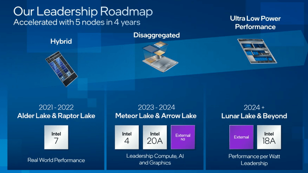
The biggest and most monumental task in Intel’s turn around is process technology. The Intel 7 to Intel 4 ramp is roughly 2 years behind TSMC and their N7 to N5 process node ramp. As mentioned earlier, Intel gets to have a period of catchup where they aren’t inventing the wheel. This should allow Intel 4 and Intel 3 to be smoother ramps.
Intel 20A is where the real test is. Intel has to deliver huge changes such as RibbonFET and PowerVia, two features that are not in volume production yet anywhere in the industry. To achieve this goal, they have introduced a new modular design architecture. They are dubbing it Tick-Tock. It appears the major front end transistor pitch scaling comes with the tick node and the tock involves optimization and further enhancements to that base.
Intel is simplifying the process flows for development and carefully considering the multivariate problem of innovation vs execution vs predictability. The tick tock model enables more independence into different segments of the process development pipeline which can be monitored and managed without impacting entire process. For example, different teams can work on signal, power delivery, and the transistor separately. The delineation and these breaks are called process modules. Each team has higher levels of accountability and this also increases the rate of learning as different features can potentially be pulled in or out.
The example Intel is offering is with PowerVia, or what the industry calls backside power delivery network. Today, across all foundries, power and signal layers are contained in a single interconnect stack. PowerVia pulls out all the power delivery and puts it on the flip side of the wafer, which enables the signal interconnects and power interconnects to be more highly optimized for the task at hand.
Intel has a custom version of their Intel 3 process node where they are testing the process flow of building the transistor layer, building the signal interconnects, bonding another to a support wafer, then flipping the combined wafer, revealing nano TSVs on the original wafer, and creating the power delivery network. This module of the process can be fully tested and debugged independently of the change in transistor architecture, RibbonFET. Active risk assessments and contingencies are in place for these high-risk process changes to ensure a delay in a module does not cause a delay for the entire process node.
Only the tock nodes are being offered within the foundry service model. Just like TSMC ramps their newest nodes such as N5 with Apple before other customers hop on, it seems Intel will do internal designs on their tick node. TSMC often has much larger waves of customers on their TSMC N5P and N4 type nodes, and this same logic applies to Intel’s tocks where their foundry customers are offered the more complete tock nodes. This is another level of de-risking for foundry customers as they will know Intel de-risked most of the node internally a year before they ramp.
Intel is ramping multiple products on Intel 4 including Meteor Lake and a custom ASIC for networking. Meanwhile, Intel 3 will ramp with 2 Xeon products which will be discussed in the datacenter section. Intel will be taping out and running test wafers in their fab for these 2024 products in the second half of this year.
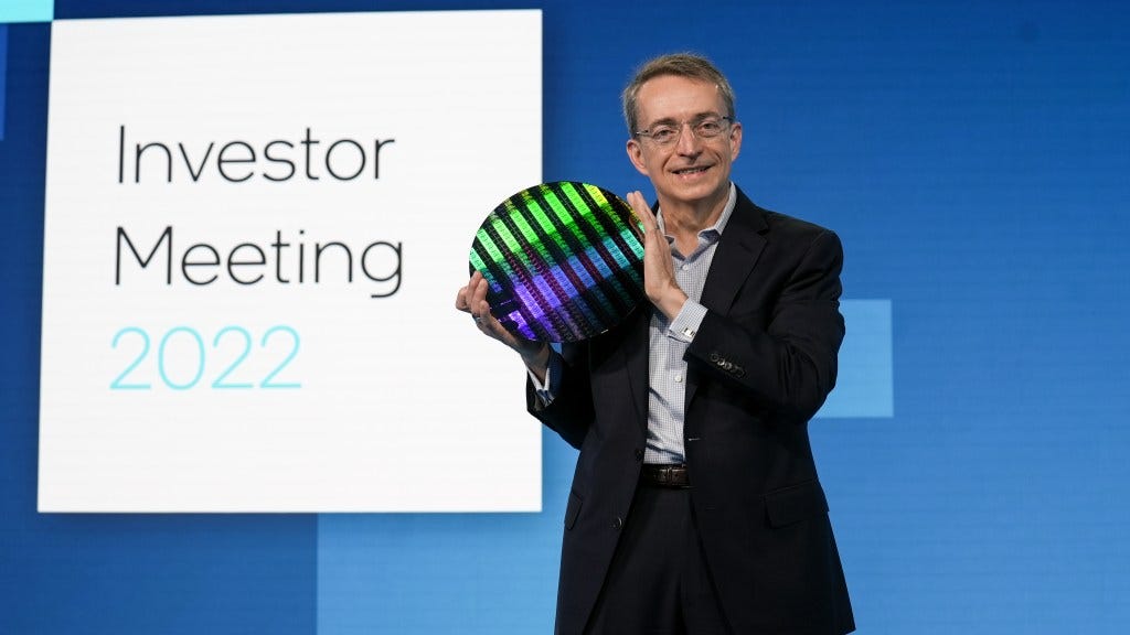
Intel is also developing 20A and 18A with different teams. These will introduce the aforementioned RibonFET, PowerVia, and High NA EUV Lithography. Intel says they are running IP test wafers for a 2024 client product in the second half of this year. 18A is going to ship foundry customers some test chip in the first half of this year, and IP shuttles in the second half. Neither of these are full chips, but they are good process for getting potential customers comfortable with the process node. Pat Gelsinger went as far as showing an 18A SRAM test wafer on stage!
There was also some information shared on packaging, but for those of you who have read our multi-part series on advanced packaging, literally nothing from the presentation is new.
Sign up to the newsletter if you would like to be informed when part 4 is released. We will be doing a deep dive on the hybrid bonding ecosystem from all the current uses, roadmaps for future generations of use, and companies involved in the supply chain from tools to IP licensing.
Intel Foundry
The foundry business is critical to Intel maintaining scale, utilization rates, and operational efficiencies. The old model of ramping a major node, then transferring most the tools to the next node was not efficient. Intel specifically mentioned with the 14nm to 10nm node transition, 90% of tools were transferable. This means 10% of the tools had to be sold as the old node ramped down. Furthermore, Intel would have to do further engineering to ensure their old tools could transfer.
In many cases, a new tool version would be released which was better suited for the task at hand, but instead of purchasing that new tool, Intel would engineer the process around the old tool. In the model of copy-exact, where the same tool and process is used across all sites in a ramp, Intel orders more of the old tool which may not be as efficient per dollar spent. We talk more about the topic in this article from last month.
In addition to the capital efficiency benefits from keeping old nodes ramped, Intel benefits by having consistently high wafer starts. In semiconductor manufacturing, utilization rates are king. A perfect example is GlobalFoundries, who Mubadala lost over $22.4B on over the course of a decade. They were plagued with low utilization rates, and now they are running at 100% utilization rates and will do so for the next few years. This single change has propelled them to becoming a profitable company and a worthwhile investment.
Intel needs the scale from a foundry business to keep pursuing the next nodes. They are large enough that the next few node transitions can be bankrolled, but eventually TSMC’s size and volumes will continue to grow, and the development costs of the bleeding edge will become too expensive to realize.
Intel’s entrance into foundry is not just diversification, but also one of necessity. The integrated design manufacture model cannot continue to forever. Intel needs to spend a lot of money to start down the path of a foundry. One of the avenues is by building more fabs. Intel says these new fabs will be paid for partially through their existing business, more debt, selling a small portion of Mobileye, government grants, and customer prepayments.
Intel also mentioned the possibility of partnering and signed MOR with Brookfield Asset Management for funding the construction of fabs. Brookfield Asset Management is an international real estate and private equity firm. They are heavily involved in many different businesses, but we believe this partnership would be designed to take advantage of investors who have pushed down rates for infrastructure and real estate lease backs to very low levels. Many firms build a headquarters, only to sell it to a company like Brookfield Asset Management and lease it back for the long term. We can certainly envision a plan where Intel builds a fab shell and sells it to Brookfield along side the terms for a multi-decade lease.
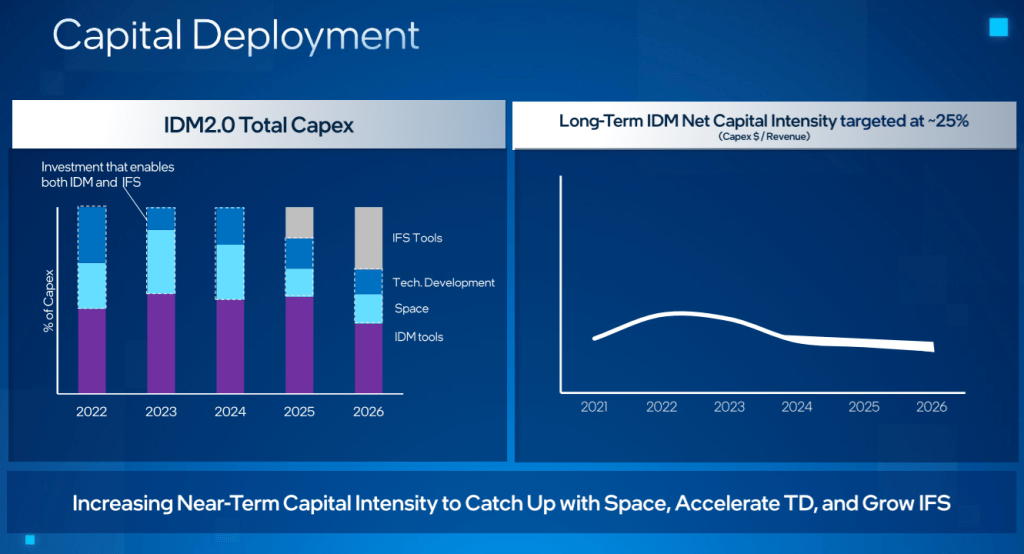
Intel’s spending is heavily heard towards technology development in 2022 relative to other years. 2022 and 2023 will include a large buildout of fab shells. These fab shells would have the option of sitting empty until needed so Intel can be more flexible in ramping capacity. Spending on tools is up in 2022 and 2023, but the juice will really come in 2025 and 2026 when the foundry business begins to spend heavily on tools.
Intel’s long-term model will include spending roughly 25% of revenue on capital expenditures. While this is lower than the 35% of 2022 and 2023, it is higher than Intel has historically spend. Capital intensity is up and that is great for firms such as Applied Materials, ASML, Lam Research, KLA, Tokyo Electron, Onto, Nova, Entegris, etc.
Intel specifically mentioned that these capital expenditure numbers are net. This means that if Intel can offset the spending via government grants and subsidies, the potential partnership with Brookfield Asset Management, and customer prepayments, their spending will only go up. Intel is conservatively penning in 10% for these offsets, but they could end up much higher if the US and EU finally recognize that they will fall completely behind in hard technology without semiconductor subsidies to match those already in place within the tax code and government budgets of countries in Asia.
Intel is talking a big game in their foundry ambitions, but SemiAnalysis has had many questions related to their entry here. Acquiring a foundry was necessary to accelerate Intel Foundry Services.
We were big believers of the strategy involved with the rumored acquisition for GlobalFoundries. Our sources indicate Intel did indeed make an offer, and Mubadala indeed turned it down due to issues with regulators and timing. Customers would not be happy with the level of information disclosure Intel would get, and the acquisition would have likely taken 18 months if it was even able to secure regulatory approval. In 18 months, the GlobalFoundries turn around would be well underway and it would be worth a good bit more than the Intel offer.
With this acquisition falling through, Intel had to turn their head to another foundry. After GlobalFoundries, UMC is the next largest, but Tawian wouldn’t allow it. SMIC is 5th and the same applies there with China. Moving down the list, Powerchip, Vanguard International Semiconductor, and Hua Hong all have these same issues. The only foundry left with reasonable volume and size was Tower Semiconductor based out of Israel.
Tower Semiconductor
The acquisition of Tower Semiconductor plugs much needed gaps in Intel's foundry offerings for process nodes beyond leading edge FinFET. Tower Semiconductor gives them teams who have been profitably running specialty technologies that interface with multiple external clients in a successful manner. Intel's biggest hole in the foundry arena is the lack of capabilities in the creation and maintenance of simple yet flexible Process Design Kit (PDK). Old Intel utilized mostly flows that were very custom tailored to their internal needs which increased development time for chip designs. This is a non-starter in the foundry business. As Intel tries to adopt more industry standard flows, PDK capabilities are an area they need a lot of help with. Towers capabilities in specialty niche technologies really boost their ability to create and offer flexible and extensible PDKs.
Tower Semiconductor offers a wide array of technology from RF CMOS, SiGe power ICs, discrete devices, CMOS image sensors, photonics, RFID, bipolar CMOS (BiCMOS), silicon-on-insulator (SOI), LDMOS transistors, MEMS, wafer bonding, Y-Flash memristors, and high-performance analog. Panasonic is Tower’s largest customer, but they have many other customers. Below is our breakdown of the technologies offered by Tower.
Silicon Photonics – Tower utilizes their SiGe BiCMOS process for integrating optical components in the datacenter communication market. The platform includes the integration of photodetectors, optical modulators, and lasers into a single die.
RF CMOS – Used in highly integrated transceivers, power amplifiers, and tuners. Integrated inductors, variable capacitors, and laterally diffused MOS transistors are all fabbed on a single die.
Silicon on Insulator (SOI) – Tower fabs antenna switches and front-end modules, commonly found in smartphones.
BiCMOS for RF – Similar to RF CMOS but more features, mostly sells into specialized trancievers and tuners. Can incorporate high-speed bipolar transistors. The equipment needs here are more specialized.
SiGe BiCMOS & Analog – Even more features than the standard BiCMOS, suited for even more advanced RF. It’s targeted at high performance analog semiconductors for high-speed, low noise, highly integrated multi-band wireless transceivers, optical networking components, automotive radars, hard drive pre-amplifiers, power amplifiers, and low noise amplifiers. Incorporates silicon germanium bipolar transistors which offers much higher performance. This process involved deep collaboration with a semiconductor capital equipment provider and is unique to Tower. They are the highest volume user of SiGe. We wonder if the engineers from Tower can assist Intel on their implementation of a SiGe channel on future leading-edge nodes.
CMOS Image Sensors and Wafer Stacking – Tower Semi CMOS image sensors are often found in Nikon cameras, but they also exist in many other high-end applications such automotive sensors and smartphones. They offer 2 main process nodes for image sensors, 110nm on 200mm wafers and 65nm on 300mm wafers with pixel sizes down to 1.12-micron. Tower is capable of dual light pipe, rolling shutter, and global shutter. Tower Semiconductor also offers backside illumination, a form of 3D eafer stacking where a digital CMOS wafer is stacked under a thinned image sensor wafer.
X-Ray and Reticle Stitching – For x-ray, Tower developed the capability to offer reticle stitching so chips can extend beyond the size of a lithography reticle. This technology is offered on the 0.18-micron node and the 65nm nodes. The x-ray chips sell into dental, CARM, angiography, mammography, and industrial non-destructive test. The x-ray sensors produced can be as large as 1 die for an entire 300mm wafer.
Other Sensors – Tower also can manufacture Infra-Red sensors for gesture recognition and spectral sensitivity sensors. They also offer indirect and direct time of flight 3D sensors for VR, AR, and smartphones. These sensors can also be used for facial recognition. Single photon avalanche diodes and LiDAR are also manufactured by Tower.
MEMS – Tower has high share within the MEMS microphone arena which is used everywhere from wireless earbuds to phones to industrial applications.
Micro-LED & Micro-OLED – Tower’s capabilities with reticle stitching also enable them to be an emerging supplier in Micro-LED for monolithic arrays in micro-OLED and LCOS displays. They are also engaged in GaN nano-tube based LEDs which can then be placed onto a backplane. This is an opportunity that Tower specifically called out as requiring more investment to scale up. We are hopeful Intel continues to invest in Tower’s Micro-LED technology.
Power Management ICs – offerings include low voltage BCD and high boltage. For low voltage, BCD is a technical advantage and includes 5V, 8V, 12V, 40V, and 60V devices for power and drive semiconductors such as voltage regulators, battery chargers, power management products, and audio amplifiers. For high-voltage, 140V Resurf, 200V SOI, and 700V technologies are offered for gat drivers for discrete high-power transistors in automotive, industrial, AC adaptors, and lighting markets.
Non-Volatile Memory – Tower developed a non volatile memory solution called Y-Flash. This can be integrated in power management products where other forms of memory will fall apart due to the strenuous conditions.
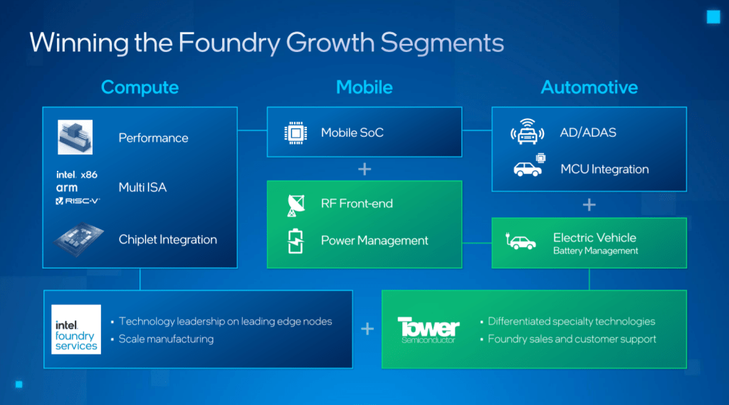
The acquisition of Tower enables Intel to offer a more complete array of technologies with which they can leverage their scale to deliver. Tower needs Intel for help with scaling their fabs for the capability to supply large verticals such as battery management systems in electric vehicles and silicon photonics. Intel gets to hit the ground with existing relationships with foundry customers and leverage those to create further engagements in Intel Foundry Services.
Tower Semi and Intel together will be focused on the segments of compute, mobile, and automotive. Intel says they are one of two foundries in the world that spans from micron level nodes all the way through sub 10nm nodes. The other is TSMC. Intel is trying to position themselves as the only competitor. This rhetoric ignores the fact that Intel with Tower still lacks heavily in the 45nm to 28nm process node range.
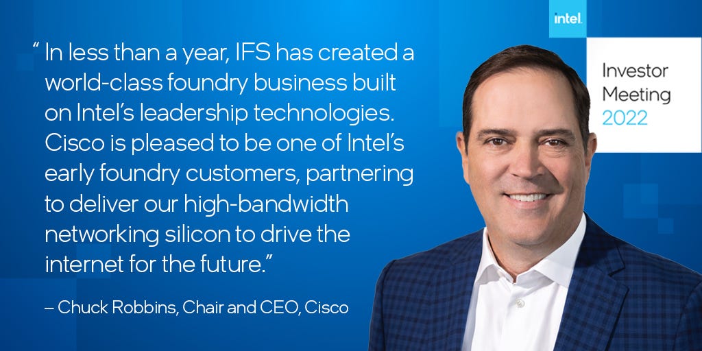
Intel is announcing another foundry customer, Cisco. Cisco Silicon One has been an interesting strategy from service provider networks with deep buffered routers to power and cost optimized web scale top of rack switches, from line cards to switches. Cisco Silicon One has been a big user of Samsung Foundry, but it looks like Intel has taken that business away. Achronix and Amazon are already customers for whom Intel ships to and collects revenue from, as we have written about in the past.
They also are the foundry contractor for the US governments RAMP C program which includes collaborations with Qualcomm, IBM, Synopsys, Cadence, and Microsoft. They claim they more than 5 “anchor prospects in design engagement” and more than 30 test chips in 2022. Intel is targeting the automotive market in ADAS, RF, sensors, and power management and even has a team within the foundry services business geared to target this business.
Intel claims that the existing foundry business was $800M in 2021. Even with business from Achronix and Amazon, this seems high. We are not sure where the rest of this revenue is coming from. Our estimate for Achronix and Amazon is still under $500M even in the most optimistic scenarios. Perhaps Intel is also capturing revenue from the department of defense already.
Datacenter And AI
Let’s be clear, Intel gets demolished in server until at least 2024 and potentially beyond. At the same time, Icelake versus Milan is as bad as it gets. Sapphire Rapids versus Genoa is still a massive gap, but the gap is not as large. Rolling forward, Emerald Rapids must fight Genoa and Bergamo. It will not be able to beat either. The most interesting thing is the 2024 products.
Granite Rapids (GNR) has been redefined yet again, as has Sierra Forest. Granite Rapids was initially a 2022 product. It was pushed to 2023 and had its capabilities tweaked. It is now a 2024 product and has had the CPU cores moved to the Intel 3 node. The same has occurred with Sierra Forest (SRF). Ever since the first redefinition, we have known they would both be part of the Birch Stream platform which utilizes the LGA7529 socket. The process node hasn’t always remained the same. It seems Intel has also move Sierra Forest from TSMC N3 to Intel 3. This is a very positive signal for internal nodes health. Regardless, Granite Rapids is not competitive with AMD’s Turin, and Sierra Forest likely doesn’t compete with Bergamo +1.
The AI segment is even worse. Habana has poor software and little to no traction. The team that Intel bought has already had to delay Habana's initial offering multiple times due to software and the 2nd generation part on TSMC N7 is also delayed to later this year instead of late last year like they initially told Intel when the purchase was made. Overall, Intel didn't do their due diligence with this purchase and it shows.
Network and Edge
This is by far the most promising business unit within Intel and the most likely to hit and exceed its revenue targets. It has by far the best competitive outlook on hardware, the most advanced use of external foundries and internal foundries where applicable including TSMC N7 for DPUs (IPUs) and Intel 4 for custom networking ASICs, and the most well-maintained software suites which rearchitect how networks are managed.. Intel’s network and edge has also most closely worked with customers for co-developed hardware platforms. Fixed function hardware is being replaced to a software programable model while also maintaining fixed function hardware where it makes sense. The network and edge group is on top of the AI Inference revolution with OpenVino.
Law of economics – It may be too expensive to bring data to cloud.
Law of physics – The workload may not have time (latency) to bring data to the cloud for your workload.
Law of the land – Regulatory or security reasons may prevent data from going to the cloud.
Intel’s networking hardware helps alleviate concerns of all 3 points, while also offering compute on the edge. Compute on the edge can often offer higher TCO. Intel has solutions targeting the cloud datacenter from silicon photonics, ethernet switches, NICs, and DPUs (IPUs). Intel is creating an open source software platform for their DPUs, which is very different from what Nvidia, Marvell, Fungible, Pensando, and Amazon are doing for their DPUs. Intel has the world’s best silicon photonics process, and co-packaged optics is their trojan horse for entering the foundry business.
Intel also has products for the core network with CPUs, NICs, and programable switches for core routers and NFV workloads. The Colocation edge includes server hosting outside of massive datacenters, and CPUs and NICs sell into this vertical. Intel also sells into the network edge with CPUs, NICs, and FlexRAN software for the RAN hub and edge compute. SnowRidge is an SOC which sells into the network edge and 5G base stations. Lastly on-premises edge includes Xeon/Atom CPUs, Movidus VPU, FPGAs, and various software such as OpenVino.
Tam is growing at 12%, but Intel expects network and edge to grow at mid-teens. They will gain share and be a huge winner on the edge. Nick McKeown is a rockstar who has had many successful companies in products in this industry. His most recent effort that was purchased by Intel, Barefoot, is ahead of its time by offering programable switches and being the first switch with co-packaged optics. We expect Intel to start eating networking switch share rapidly in the >100Tbps switch era. Pat Gelsinger seems to indicate he had to woo him to lead the group, and it’s a blessing for Intel that they have him.
Accelerated Computing and Graphics
While we are super optimistic on the network and edge group, we are not optimistic at all on AXG. They have to build a massive software suite, and while OneAPI has already surpassed AMD’s GPU software, it’s nowhere close to Nvidia’s. The Xeon products with HBM are only useful in very small niches. The GPU IP has a long way to go and fighting both Nvidia and AMD is going to be really difficult. Furthermore, Intel is using external nodes for their gaming GPUs, so they cannot use the IDM advantage to compete on cost either. Their worse architecture will show through directly to die sizes and BOM.
It doesn’t help that Intel’s slide were somewhat deceptive. Anyone get excited about the 4M units of GPUs shipped in 2022 and the >$1B revenue figure? Yea we were too, initially… until we started looking at fine print.
Do you see it?
AXG revenue includes intersegment graphics royalty that is eliminated in Intel consolidated results. This royalty is approximately $700M in 2021, growing to approximately $1B in 2026.
In reality, Intel expects to ship 4 million GPU units, but only earn $300M revenue on it with the rest being intra company royalties that are just made up?
That’s a ~$75 average selling price.
Is Intel just selling low end GPUs to get market share?
They have 2 dies which they will sell, and the smaller of the two is only 128 execution units. For reference, the last generation Tiger Lake integrated GPU was 96 execution units, and next generation Meteor Lake goes up to 192 execution units. The vast majority of Intel’s GPU volume will sell into the market at ~$75 or less ASPs and offer worse performance than AMD’s integrated graphics and worse than Intel’s next generation iGPU as well.
The only out we can see is Intel’s claim of 4M units shipped doesn’t mean shipped for revenue. For the first generation of discrete GPUs, Intel could potentially be switching to the super market model where they do not get paid until the ODM sells the laptop or GPU through to the end user or channel. This would be pretty smart because then Intel can stuff the channel with their inferior GPUs, and ODMs take no risk on their balance sheet if they do not sell. They would even be incentivized to sell Intel GPUs due to the amazing return on invested capital that they get.
We respect Raja Koduri, the leader of Intel’s AXG, but he has a very difficult path ahead of him on executing here. He was handed the worst iGPU architecture in the industry including comparing against Nvidia, AMD, Arm, Imagination, Qualcomm, and Apple. He was then asked to make magic out of it. Eventually we hope Intel’s AXG gets up to snuff, but we see no reason for AXG to be able to hit $10B of revenue in 2026, even with $1B of intra-company licensing revenue.
The only positives here are the AV1 encoding GPU and blockchain accelerator which look really nice. We aren’t crypto people, but we do track performance, network sizes, hashing power, and semi demand closely. The custom design services could be successful, but there’s a massive question mark here about what sort of semicustom deals could sit here.
Falcon Shores is an interesting and ambitious product, which combines GPU and CPU on the same carrier, but it will be later than Nvidia’s Grace Hopper and AMD’s next generation HPC processor.
Client
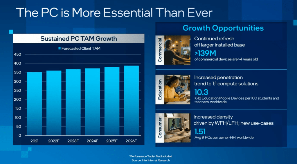
And it goes from bad to worse here. Intel’s client group is their largest, but some of the projections here are very questionable. Intel projected PC units to be above 350M in 2022 and continue to grow from that number in years ahead. Just to be clear, no analyst or market research firm is projecting PC units to continue to remain so high. Even AMD has 2022 as flat for total units. Most have 2022 as flat at 350M units, then a return to equilibrium. Intel’s data is very non-consensus. These feed into their financials by the way...
As far as competitiveness, Intel’s roadmaps on mobile are somewhat competitive. They aren’t dominating AMD like they claim with Alder Lake, but there is decent competition. We expect the performance lead to flip flop back and forth for AMD and Intel.
Software and Mobileye
This piece is already quite long, and while we have done a lot of work on these two components in the past and continue to do so, we won’t include it in the article. Mobileye and their go public offering will be fun. We like the firm, but it will depend on valuation. On software, the software unit did a little over $100M revenue last year and are targeting $150M this year. The software is even more critical because it feeds into sales for AXG, datacenter, and network and edge.
Our analysis of the financial guidance will be behind the subscriber only wall, including whether or not we think Intel is worth buying. We also discuss the foundry business and potential wins a little bit.


